Electronic component and substrate module
A technology of electronic components and substrate modules, which is applied to components with fixed capacitance, printed circuits connected with non-printed electrical components, laminated capacitors, etc., and can solve problems such as the short circuit of the laminated capacitor 500 and the solder connection of the external electrodes 514 , to achieve low ESL and suppress short circuit
- Summary
- Abstract
- Description
- Claims
- Application Information
AI Technical Summary
Problems solved by technology
Method used
Image

Examples
no. 1 approach
[0060] (Structure of Electronic Components)
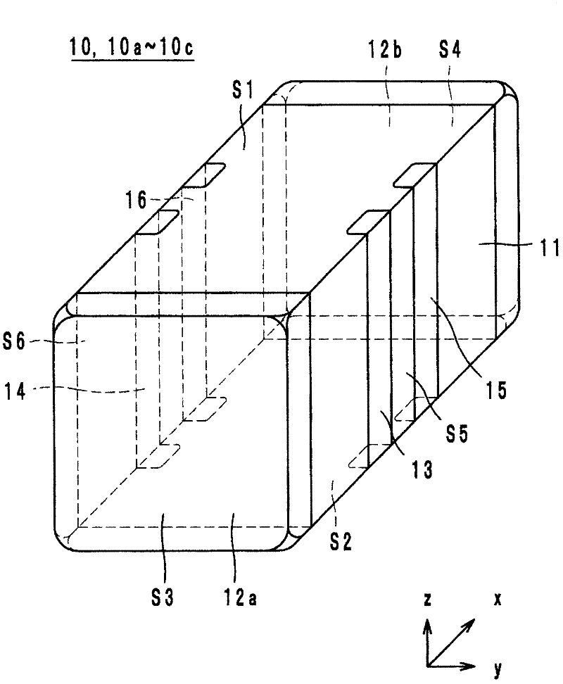
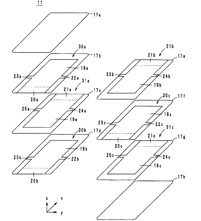
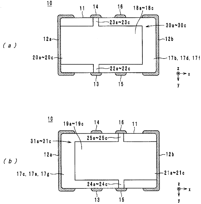
[0061] First, the configuration of the electronic component of the first embodiment will be described with reference to the drawings. figure 1 It is an external perspective view of the electronic component 10 of 1st Embodiment. figure 2 yes figure 1 An exploded perspective view of the laminated body 11 of the electronic component 10 of . image 3 yes figure 1 Internal top view of electronic components. Hereinafter, the lamination direction of the laminated body 11 is defined as the z-axis direction. When the laminated body 11 is planarly viewed from the z-axis direction, the direction in which the long side of the laminated body 11 extends is defined as the x-axis direction. When the laminated body 11 is planarly viewed from the z-axis direction, the direction in which the short side of the laminated body 11 extends is defined as the y-axis direction.
[0062] The electronic part 10 is, for example, a chip capacitor used ...
no. 2 approach
[0149] Hereinafter, the configuration of the electronic component 10a of the second embodiment will be described with reference to the drawings. Figure 12 It is an exploded perspective view of the laminated body 11a of the electronic component 10a of 2nd Embodiment. Figure 13 yes Figure 12 An internal top view of the electronic component 10a. In addition, the external perspective view of the electronic component 10a is the same as the external perspective view of the electronic component 10, so figure 1 .
[0150] Such as Figure 12 As shown, the laminated body 11 a further has a ceramic layer 17 i and internal conductors 41 , 42 .
[0151] Such as Figure 12 As shown, the ceramic layer 17i is disposed between the ceramic layer 17a and the ceramic layer 17b. The inner conductors 41 and 42 are provided on the surface of the ceramic layer 17i, and are arranged in order from the negative direction side to the positive direction side in the x-axis direction with gaps the...
no. 3 approach
[0162] Hereinafter, the structure of the electronic component 10b of 3rd Embodiment is demonstrated, referring drawings. Figure 14 It is an internal plan view of the electronic component 10b of 3rd Embodiment. In addition, the external perspective view of the electronic component 10b is the same as the external perspective view of the electronic component 10, so figure 1 .
[0163] Such as Figure 14 As shown, the electronic component 10 b is different from the electronic component 10 in that the lead conductors 23 and 25 are not provided. In this case, the electronic component 10 b is mounted so that the side surface S5 faces the circuit board 51 . External electrodes 13 to 16 are not provided on upper surface S1 and lower surface S2 of electronic component 10 . Therefore, the width in the z-axis direction of the electronic component 10 can be reduced. As a result, the electronic components 10 can be arranged close to each other.
PUM
| Property | Measurement | Unit |
|---|---|---|
| Thickness | aaaaa | aaaaa |
| Thickness | aaaaa | aaaaa |
| Thickness | aaaaa | aaaaa |
Abstract
Description
Claims
Application Information
 - R&D Engineer
- R&D Manager
- IP Professional
- Industry Leading Data Capabilities
- Powerful AI technology
- Patent DNA Extraction
Browse by: Latest US Patents, China's latest patents, Technical Efficacy Thesaurus, Application Domain, Technology Topic.
© 2024 PatSnap. All rights reserved.Legal|Privacy policy|Modern Slavery Act Transparency Statement|Sitemap