Multi-layered circuit board and semiconductor device

a multi-layer circuit board and semiconductor technology, applied in the direction of semiconductor/solid-state device details, cross-talk/noise/interference reduction, printed circuit non-printed electric components association, etc., can solve the problem of degrading the high-frequency characteristics of the multi-layered circuit board

Inactive Publication Date: 2018-12-04
NODA SCREEN
View PDF18 Cites 1 Cited by
  • Summary
  • Abstract
  • Description
  • Claims
  • Application Information

AI Technical Summary

Benefits of technology

[0020]According to the present invention, an ESL of a capacitor component including lead wirings is maintained low because magnetic field generated by a current is canceled.

Problems solved by technology

As a result, high-frequency characteristics of the multi-layered circuit board degrade.

Method used


Image

  • Multi-layered circuit board and semiconductor device
  • Multi-layered circuit board and semiconductor device
  • Multi-layered circuit board and semiconductor device

Examples


first embodiment

[0046]the present invention will be described with reference to FIGS. 1 to 18.

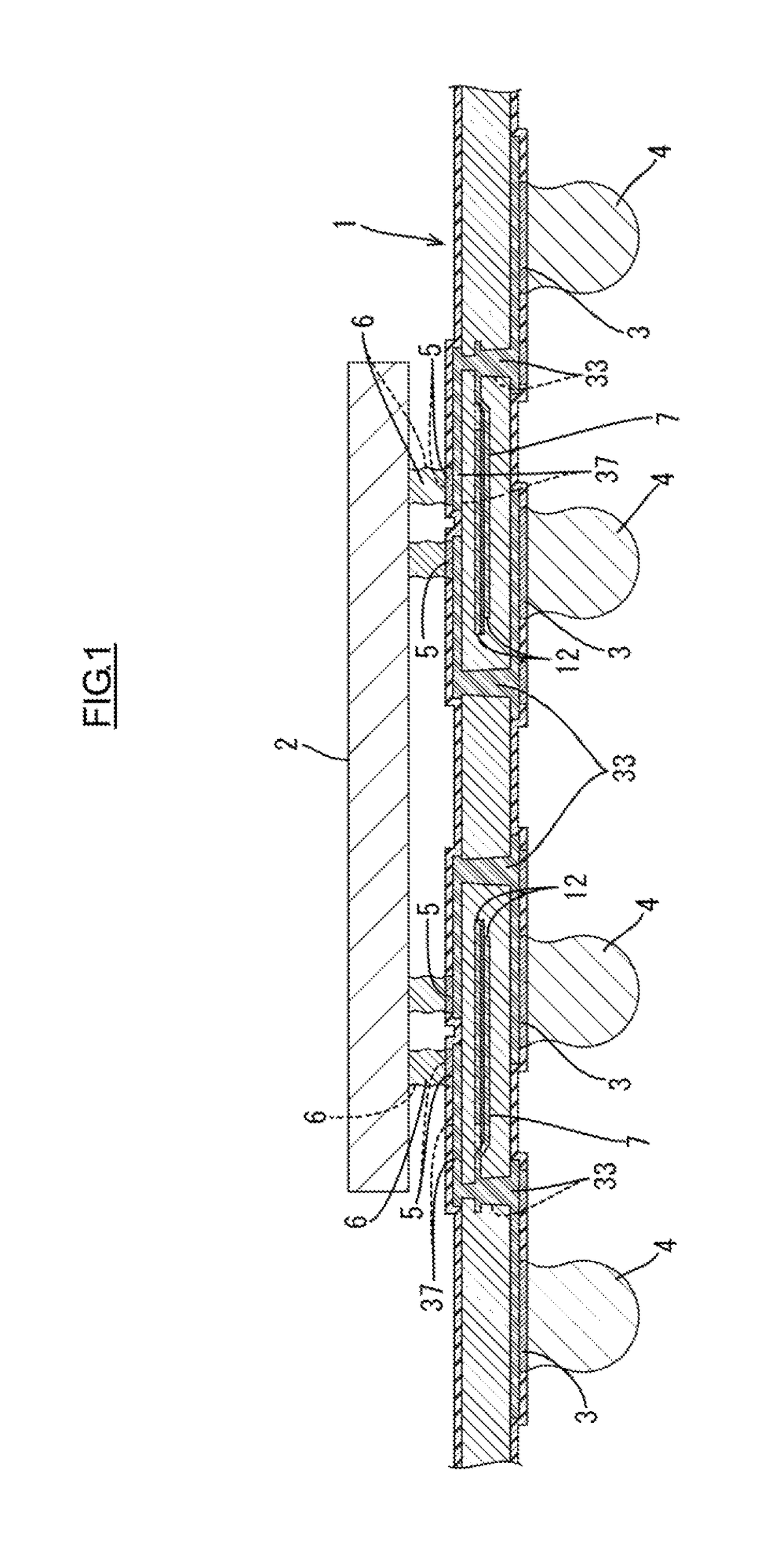
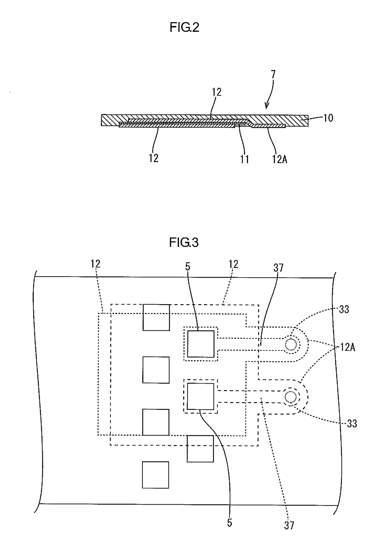
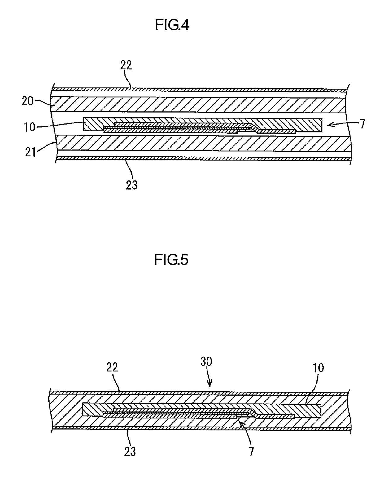
[0047]A package including an LSI 2 and a multi-layered circuit board 1 that is used as a relay board according to the first embodiment is illustrated in FIG. 1. External connection pads 3 are formed on a lower surface of the multi-layered circuit board 1. Solder balls 4 for external connection are formed on the external connection pads 3. Chip connecting pads5 are formed on an upper surface of the multi-layered circuit board 1 at positions corresponding to pads of the LSI 2, which are not illustrated. The multi-layered circuit board 1 is connected to the LSI 2 with micro solder balls 6 formed on the chip connecting pads 5. The multi-layered circuit board 1 includes sheet capacitors 7 therein. The sheet capacitors 7 are located between multiple pairs of power supply terminals and ground terminals of the LSI 2. The sheet capacitors 7 function as bypass capacitors. The chip connecting pads 5 are an example of...


PUM


Abstract

A multi-layered circuit board includes a first insulating layer, a second insulating layer, and a sheet capacitor that is located between the first insulating layer and the second insulating layer. The sheet capacitor includes a pair of electrodes that sandwich a dielectric. Lead wirings continue to the electrodes, respectively. The lead wirings are disposed on an opposite side of the first or the second insulating layer with respect to the sheet capacitor to overlap the electrodes when viewed from a stacking direction of the multi-layered circuit board. Because the lead wirings are arranged to overlap the electrodes in the stacking direction of the multi-layered circuit board, an ESL of the sheet capacitor is maintained low.

Description

TECHNICAL FIELD[0001]The present invention relates to a multi-layered circuit board including capacitors and a semiconductor deviceBACKGROUND ART[0002]A multi-layered circuit board is produced by stacking insulating layers on surfaces of which wiring patterns are formed with copper foils or other materials. When the multi-layered circuit board is used as a mounting board for mounting electronic components thereon such as semiconductor chips, a capacitor that functions as a bypass capacitor may be included in the multi-layered circuit board. An equivalent series inductance (ESL) of such a capacitor increases proportional to a length of wiring between the capacitor and the electronic component. As a result, high-frequency characteristics of the multi-layered circuit board degrade. A technology to resolve such a problem by enclosing the capacitor between insulating layers and arranging the capacitor adjacent to the electronic component has been known.RELATED ART DOCUMENTPatent Document...

Claims


Application Information

Patent Timeline
Patent Type & Authority Patents(United States)
IPC IPC(8): H05K1/18H05K1/02H05K1/11H05K1/16H01L23/498H01L23/00
CPCH05K1/0231H01L23/49822H01L23/49838H01L24/17H05K1/0298H05K1/11H05K1/113H05K1/162H05K1/181H05K1/185H05K2201/09672H01L23/49816H01L23/49827H01L24/13H01L24/16H01L2224/131H01L2224/16227H01L2224/16235H01L2924/15311H01L2924/15747H01L2924/19011H01L2924/19041H01L2924/014
Inventor OYAMADA, SEISEIYOSHIZAWA, MASAMITSU
Owner NODA SCREEN
Why Eureka
Try Eureka