ESD protection device

a protection device and shielding technology, applied in semiconductor devices, semiconductor/solid-state device details, diodes, etc., can solve problems such as failure to solve problems, failure to protect a semiconductor integrated circuit from surge, and increase the clamp voltage, so as to reduce the current pathway, suppress the generation of esl, and reduce the current current path

Active Publication Date: 2015-12-17
MURATA MFG CO LTD
View PDF7 Cites 3 Cited by
  • Summary
  • Abstract
  • Description
  • Claims
  • Application Information

AI Technical Summary

Benefits of technology

[0012]In this configuration, when currents flow through the two diodes, the current flow in directions opposite to each other, and magnetic fields generated by the current flows thus cancel each other out. For this reason, the inductance of the current pathway is reduced, and lower ESL can be achieved.
[0013]According to the present invention, the shortened current pathway of the ESD protection device can suppress the generation of ESL and keeps the clamp voltage low.

Problems solved by technology

Such semiconductor integrated circuits are low-voltage drive circuits composed of micro wiring patterns formed on semiconductor substrates, and thus generally fragile against electrostatic discharge such as surge.
In particular, in the case of using an ESD protection circuit in the high-frequency band, the clamp voltage is increased as the ESL is increased, and there are thus problems such as failure to protect a semiconductor integrated circuit from surge.
This problem is not able to be solved by Patent Document 1.

Method used


Image

  • ESD protection device
  • ESD protection device
  • ESD protection device

Examples


Embodiment Construction

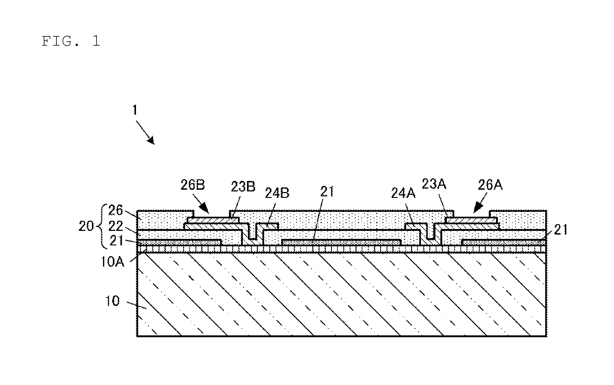
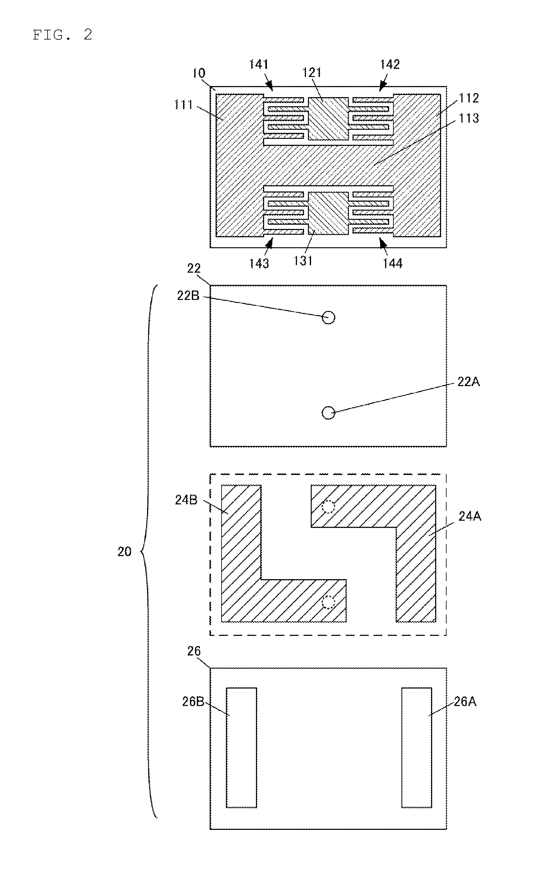
[0029]FIG. 1 is a front cross-sectional view of an ESD protection device 1 according to the present embodiment. FIG. 2 is a plan view of respective layers of the ESD protection device 1. The ESD protection device 1 is a CSP (Chip Size Package) type device, where a rewiring layer 20 including multiple resin layers, etc. is formed on a Si substrate 10. The Si substrate 10 has a rectangular shape with long sides and short sides in planar view, and has an ESD protection circuit 10A configured to include diodes and a zener diode. While the Si substrate 10 corresponds to a semiconductor substrate according to the present invention, the semiconductor substrate according to the present invention is not limited to any Si substrate, but may be a GaAs substrate or the like.

[0030]FIG. 3 is a diagram illustrating the ESD protection circuit 10A formed on the Si substrate 10.

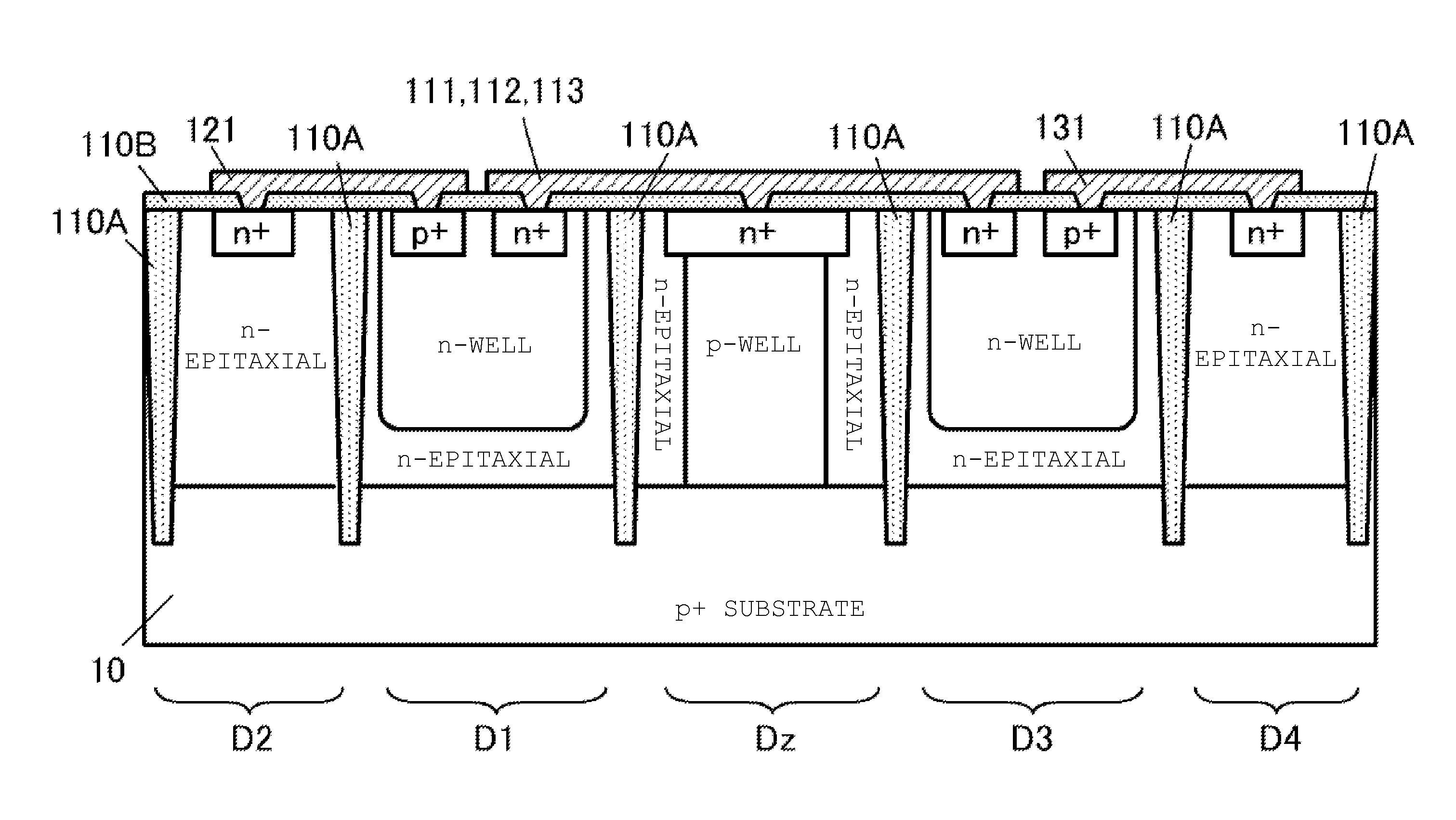
[0031]FIG. 4 is a diagram illustrating a structure example of the ESD protection circuit 10A.

[0032]As shown in FIG. 2, the S...


PUM


Abstract

An ESD protection device includes a zener diode, and a series circuit of diodes and a series circuit of diodes that are connected in parallel with the zener diode. At the connection point between the diodes, an Al electrode film is formed on the surface of a Si substrate, and at the connection point between diodes, an Al electrode film is formed on the surface of the Si substrate. The diodes are formed on the surface of the Si substrate, and the diodes are formed in the thickness direction of the Si substrate. The Si substrate has a longitudinal direction and a shorter direction orthogonal to the longitudinal direction in planar view, and the Al electrode films are formed respectively at both ends in the shorter direction of the Si substrate. Thus, provided is an ESD protection device which suppresses the ESL, and keeps the clamp voltage low.

Description

CROSS REFERENCE TO RELATED APPLICATIONS[0001]The present application is a continuation of PCT / JP2014 / 054404 filed Feb. 25, 2014, which claims priority to JP Application No. 2013-149004, filed Jul. 18, 2013, JP Application No. 2013-126659, filed Jun. 17, 2013, JP Application No. 2013-115676, filed May 31, 2013, JP Application No. 2013-097494, filed May 7, 2013, JP Application No. 2013-079960, filed Apr. 5, 2013, JP Application No. 2013-079978, filed Apr. 5, 2013, and JP Application No. 2013-039379, filed Feb. 28, 2013, the entire contents of each of which are incorporated herein by reference.FIELD OF THE INVENTION[0002]The present invention relates to an ESD protection device which protects an electronic circuit from electrostatic discharge.BACKGROUND OF THE INVENTION[0003]ESD (Electro-Static-Discharge) protection devices can be a type of semiconductor devices. The ESD protection device protects semiconductor ICs, etc. from static electricity, etc. Various electronic devices includin...

Claims


Application Information

Patent Timeline
Patent Type & Authority Applications(United States)
IPC IPC(8): H01L27/02H01L27/08H01L23/528H01L29/866
CPCH01L27/0255H01L23/528H01L27/0814H01L29/866H01L29/8611H01L29/8613H01L2224/16
Inventor KATO, NOBORUNAKAISO, TOSHIYUKI
Owner MURATA MFG CO LTD
Why Eureka
Try Eureka