Electronic component

a technology of electronic components and components, applied in the field of electronic components, can solve the problems of water or the like being difficult to enter the electronic component body, and achieve the effects of improving the reliability of the electronic component, low esl, and large capacitan

Active Publication Date: 2017-08-10
MURATA MFG CO LTD
View PDF5 Cites 2 Cited by
  • Summary
  • Abstract
  • Description
  • Claims
  • Application Information

AI Technical Summary

Benefits of technology

[0017]In an electronic component according to a preferred embodiment of the present invention, it is preferred that the first internal electrode includes a first opposing portion opposite to the second internal electrode in the laminating direction; the second internal electrode includes a second opposing portion opposite to the first internal electrode in the laminating direction; and a distance in the length direction between the first and the second opposing portions and the first or the second end surface is about 10 μm or more and about 70 μm or less, for example. By setting the distance in the length direction between the first and the second opposing portions and the first or the second end surface to be about 10 μm or more, it is possible to improve the reliability of the electronic component. By setting the distance in the length direction between the first and the second opposing portions and the first or the second end surface to be about 70 μm or less, it is possible to realize a large capacitance and a low ESL, for example, when the electronic component is a capacitor.
[0018]In an electronic component according to a preferred embodiment of the present invention, it is preferred that the first internal electrode includes a first opposing portion opposite to the second internal electrode in the laminating direction; the second internal electrode includes a second opposing portion opposite to the first internal electrode in the laminating direction; and a distance in the width direction between the first and the second opposing portions and the first or the second lateral surface is about 10 μm or more and about 70 μm or less, for example. By setting the distance in the width direction between the first and the second opposing portions and the first or the second lateral surface to be about 10 μm or more, it is possible to improve the reliability of the electronic component. By setting the distance in the width direction between the first and the second opposing portions and the first or the second lateral surface to be about 70 μm or less, it is possible to realize a large capacitance and a low ESL, for example, when the electronic component is a capacitor.
[0019]According to various preferred embodiments of the present invention, it is possible to provide electronic components having excellent reliability.

Problems solved by technology

Therefore, the end portions of the electronic component body where the water or the like is likely to enter the electronic component body are covered with the thick external electrodes, and thus the water or the like is difficult to enter the electronic component body.

Method used


Image

  • Electronic component
  • Electronic component
  • Electronic component

Examples


first preferred embodiment

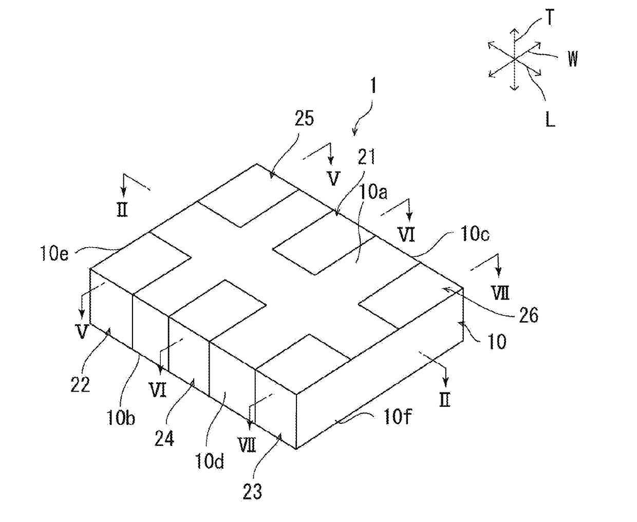
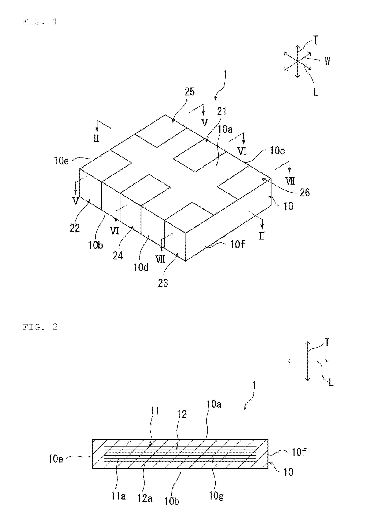
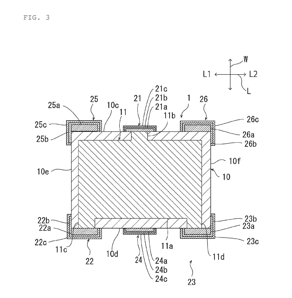
[0036]FIG. 1 is a schematic perspective view of a capacitor according to a first preferred embodiment of the present invention. FIG. 2 is a schematic section view along line II-II in FIG. 1. FIG. 3 is a schematic section view of the capacitor according to the first preferred embodiment. FIG. 4 is a schematic section view of the capacitor according to the first preferred embodiment. FIG. 5 is a schematic section view along line V-V in FIG. 1. FIG. 6 is a schematic section view along line VI-VI in FIG. 1. FIG. 7 is a schematic section view along line VII-VII in FIG. 1.

[0037]As shown in FIG. 1 to FIG. 7, a capacitor 1 includes a capacitor body (electronic component body) 10. The capacitor body 10 preferably has a rectangular or substantially rectangular parallelepiped shape. The capacitor body 10 includes a first and a second principal surfaces 10a, 10b, a first and a second lateral surfaces 10c, 10d, and a first and a second end surfaces 10e, 10f. Each of the first and the second prin...

second preferred embodiment

[0088]FIG. 8 is a schematic perspective view of a capacitor according to a second preferred embodiment of the present invention. A capacitor 1a in FIG. 8 is different from the capacitor 1 according to the first preferred embodiment in that the external electrodes 22, 23, 25, 26 located on the outermost side in the length direction L cover the ridge defined by the first or the second lateral surface 10c, 10d and the principal surface 10a, the ridge defined by the first or the second lateral surface 10c, 10d and the second principal surface 10b, and the ridge defined by the first or the second lateral surface 10c, 10d and the first or the second end surface 10e, 10f. Specifically, each of the external electrodes 22, 25 disposed on the L1 side in the length direction L covers the ridge defined by the first or the second lateral surface 10c, 10d and the principal surface 10a, the ridge defined by the first or the second lateral surface 10c, 10d and the second principal surface 10b, and ...

third preferred embodiment

[0090]FIG. 9 is a schematic plan view of a capacitor according to a third preferred embodiment of the present invention. FIG. 10 is a schematic section view of the capacitor according to the third preferred embodiment. FIG. 11 is a schematic section view of the capacitor according to the third preferred embodiment.

[0091]As shown in FIG. 9, in a capacitor 1b according to the present preferred embodiment, four or more external electrodes 20a are disposed on the first lateral surface 10c, and four or more external electrodes 20b are disposed on the second lateral surface 10d. Among the plurality of external electrodes 20a, external electrodes 20a1, 20a2 located on the outer side in the length direction L are thicker than the other external electrodes 20a. Among the plurality of external electrodes 20b, external electrodes 20b1, 20b2 located on the outer side in the length direction L are thicker than the other external electrodes 20b.

[0092]Also, one of the external electrode 20a1 loca...


PUM

PropertyMeasurementUnit
lengthaaaaaaaaaa
lengthaaaaaaaaaa
widthaaaaaaaaaa

Abstract

An electronic component having excellent reliability includes a first lateral surface and two external electrodes on an outermost side in a length direction among three or more external electrodes on the first lateral surface that are thicker than the other external electrode. On a second lateral surface, two external electrodes that are located on the outermost side in the length direction among three or more external electrodes disposed on the second lateral surface are thicker than the other external electrode.

Description

CROSS REFERENCE TO RELATED APPLICATIONS[0001]This application claims the benefit of priority to Japanese Patent Application No. 2016-022550 filed on Feb. 9, 2016. The entire contents of this application are hereby incorporated herein by reference.BACKGROUND OF THE INVENTION[0002]1. Field of the Invention[0003]The present invention relates to an electronic component.[0004]2. Description of the Related Art[0005]Recently, various semiconductor devices such as large-scale integrated circuits (LSI) have been used in information devices and the like. A semiconductor device is provided with a power circuit for supplying electric power. When a high-frequency wave is generated in association with the switching of the power source or the clock operation in the power circuit, the operation of the semiconductor device can become unstable. Therefore, it is preferred to use a capacitor having a low equivalent series inductance (ESL) in a power circuit so as to prevent the generation of a high-fre...

Claims


Application Information

Patent Timeline
Patent Type & Authority Applications(United States)
IPC IPC(8): H01G4/30H01G4/232H01G4/012
CPCH01G4/30H01G4/2325H01G4/012H01G4/005H01G4/12H01G4/35H01G4/232
Inventor NAKAZAWA, HIROTAKASAWADA, TAKASHI
Owner MURATA MFG CO LTD
Why Eureka
Try Eureka