Wiring board and display apparatus

一种配线基板、配线的技术,应用在辨认装置、静态指示器、非线性光学等方向,能够解决迂回配线电短路、变窄等问题

Inactive Publication Date: 2012-09-12
SHARP KK
View PDF8 Cites 9 Cited by
  • Summary
  • Abstract
  • Description
  • Claims
  • Application Information

AI Technical Summary

Problems solved by technology

[0004] With narrower frames, in the area where routing wires are provided (frame area), the distance between adjacent routing wires tends to be narrowed, and electrical short circuits between routing wires tend to occur.

Method used


Image

  • Wiring board and display apparatus
  • Wiring board and display apparatus
  • Wiring board and display apparatus

Examples


Embodiment approach 1

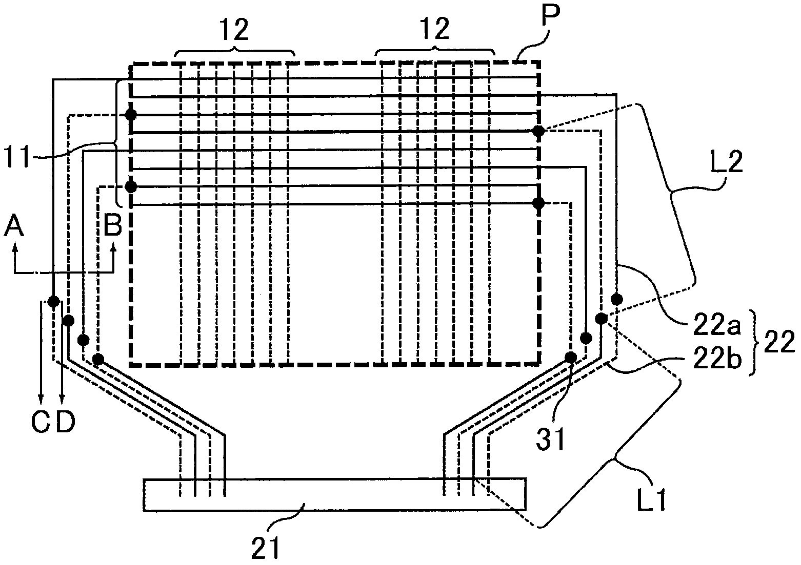
[0062] Embodiment 1 is an example of the active matrix substrate (wiring substrate) of the present invention that can be used as a substrate constituting a liquid crystal display panel. figure 1 It is a schematic plan view showing the wiring structure of the active matrix substrate of the first embodiment. Such as figure 1 As shown, in the active matrix substrate of Embodiment 1, a plurality of gate wirings 11 and a plurality of source wirings 12 are provided in a display region (control region) P. As shown in FIG. The plurality of gate wirings 11 extends in the row direction, and the plurality of source wirings 12 extends in the column direction.

[0063] In addition, a TFT as a switching element is arranged at a position adjacent to each intersection of the plurality of gate lines 11 and the plurality of source lines 12 , and the TFT is connected to the pixel electrode. The pixel electrode is an electrode provided in a region (pixel) surrounded by the gate wiring 11 and ...

Embodiment approach 2

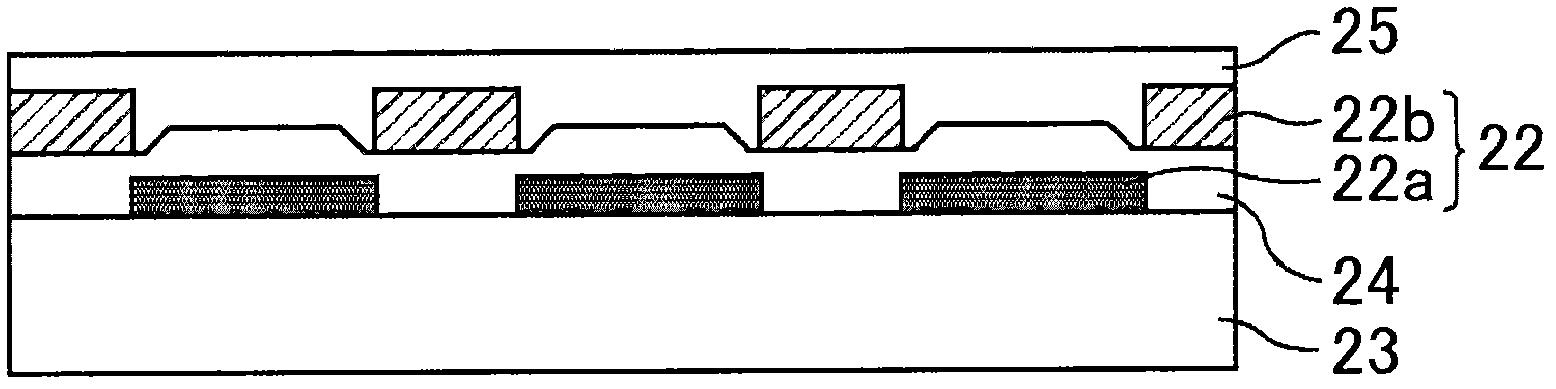
[0090] Embodiment 2 is an example of the active matrix substrate (wiring substrate) of the present invention that can be used as a substrate constituting a liquid crystal display panel. The active matrix substrate of Embodiment 2 is the same as the active matrix substrate of Embodiment 1 except that the source wiring includes a gate metal portion and a source metal portion.

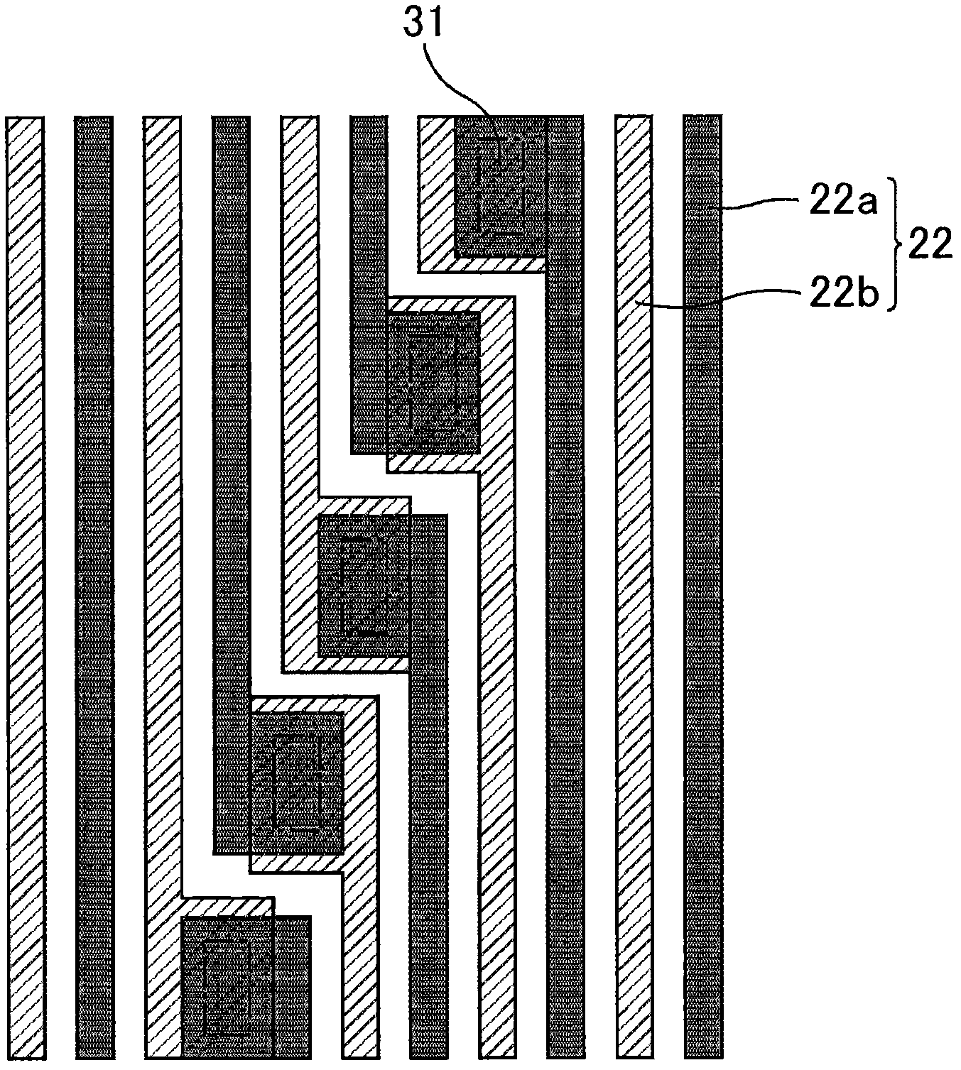
[0091] Figure 6 It is a schematic plan view showing the wiring structure of the active matrix substrate of the second embodiment. Such as Figure 6 As shown, in the active matrix substrate of Embodiment 2, a plurality of gate wirings 11 and a plurality of source wirings 12 are arranged in a display region (control region) P. As shown in FIG. The plurality of gate wirings 11 extends in the row direction, and the plurality of source wirings 12 extends in the column direction. A plurality of routing lines 42 of different materials are sequentially and alternately drawn out from the gate driver 41 , and a...


PUM


Abstract

Disclosed is a wiring board wherein the resistance difference among a plurality of drawn wiring lines is reduced. The wiring board has: a control region, which includes a plurality of gate wiring lines extending in the row direction, and a plurality of source wiring lines extending in the column direction; and a peripheral region, which includes a gate driver connected to the gate wiring lines, a source driver connected to the source wiring lines, and a plurality of drawn wiring lines, which are drawn along the outer periphery of the control region and connect the gate driver and the gate wiring lines. Each of the drawn wiring lines has a gate metal portion configured of the material of the gate wiring lines, and a source metal portion configured of the material of the source wiring lines. An insulating layer is disposed between the gate metal portion and the source metal portion, and the gate metal portion and the source metal portion are connected to each other through a contact section that penetrates the insulating layer.

Description

technical field [0001] The present invention relates to a wiring board and a display device. More specifically, it relates to a wiring board suitable for use as a substrate constituting a panel of a display device, and a display device including the wiring board. Background technique [0002] In recent years, portable electronic devices such as mobile phones and PDAs equipped with liquid crystal display panels, organic electroluminescent display panels, and the like have been required to further reduce their size and weight. Along with this, there is a tendency to reduce the size of the periphery of the display area, that is, to narrow the frame, and development is being actively carried out. [0003] In these electronic devices, in order to perform high-definition display, a plurality of gate wirings (scanning signal lines) and a plurality of source wirings (image signal lines) are provided in a display region. Furthermore, the plurality of gate wirings are driven by a ga...

Claims


Application Information

Patent Timeline
Patent Type & Authority Applications(China)
IPC IPC(8): G09F9/30G02F1/1345H05K1/02
CPCH05K1/0289G02F1/13452G09G3/2092H05K2201/10136
Inventor 森纯一
Owner SHARP KK
Why Eureka
Try Eureka