Pixel cell driving circuit, pixel cell driving method, pixel cell and display device

A pixel unit and drive circuit technology, applied in the field of pixel unit drive circuits, pixel units and display devices, can solve the problems of different drive currents, poor brightness uniformity, panel brightness differences, etc., and achieve the effect of improving brightness unevenness

Active Publication Date: 2012-10-03
BOE TECH GRP CO LTD +1
View PDF4 Cites 35 Cited by
  • Summary
  • Abstract
  • Description
  • Claims
  • Application Information

AI Technical Summary

Problems solved by technology

The driving current formula of the 2T1C circuit includes Vth. As mentioned above, due to the immaturity of the LTPS process, even with the same process parameters, the Vth of the TFTs at different positions on the manufactured panel is quite different, resulting in the same gray area. The driving current of OLED is different under the step voltage, so the brightness of different positions of the panel under this driving scheme will be different, and the brightness uniformity is poor.

Method used


Image

  • Pixel cell driving circuit, pixel cell driving method, pixel cell and display device
  • Pixel cell driving circuit, pixel cell driving method, pixel cell and display device
  • Pixel cell driving circuit, pixel cell driving method, pixel cell and display device

Examples


Embodiment Construction

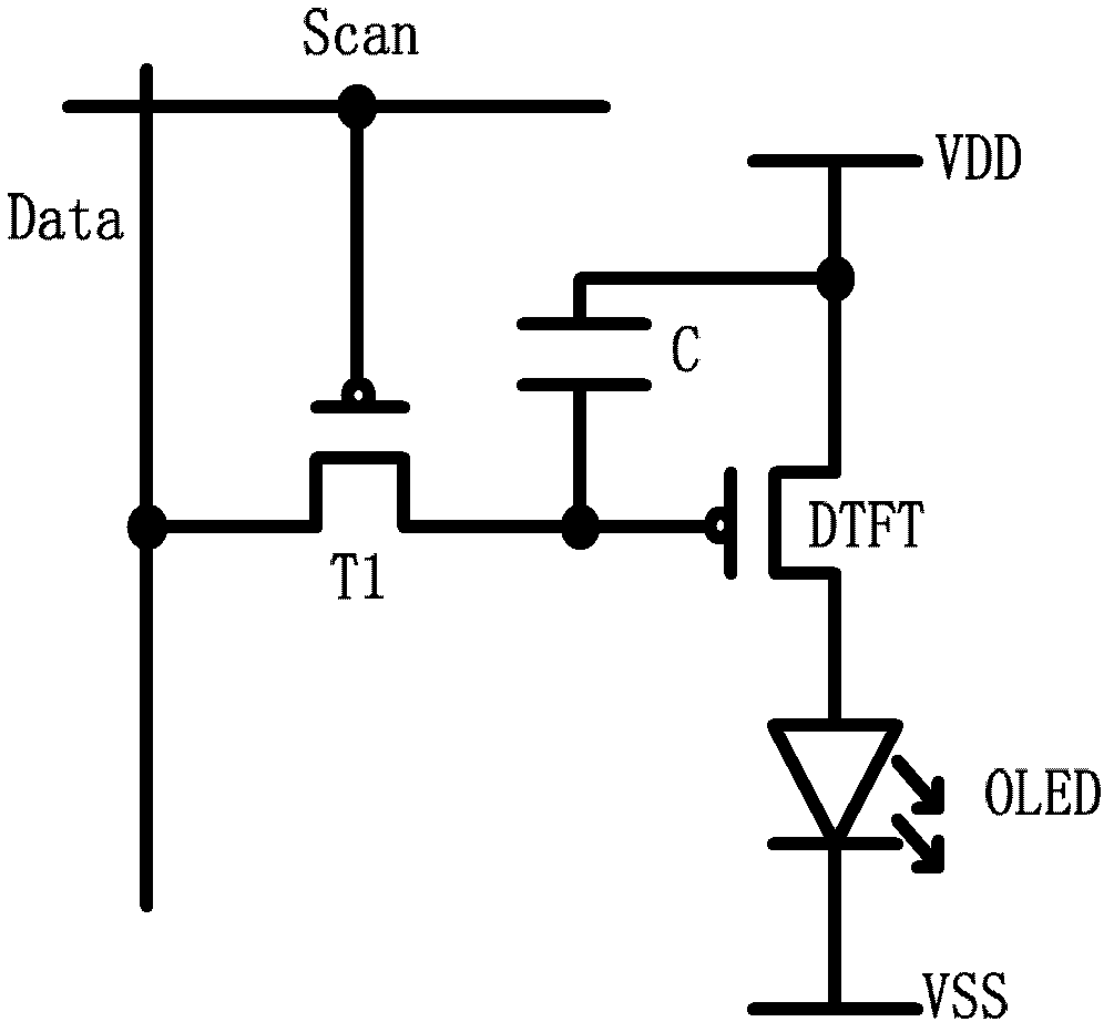
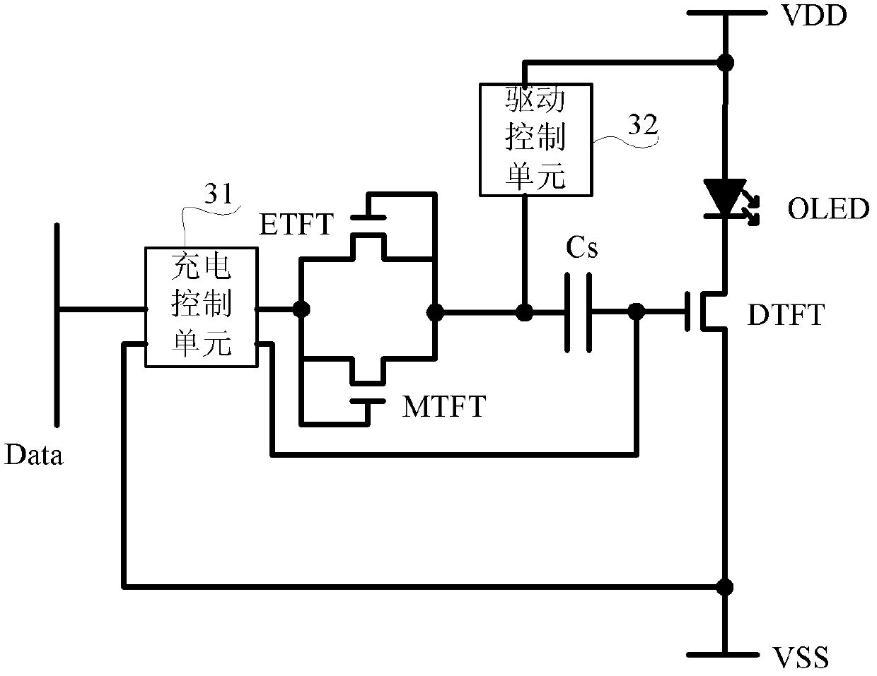
[0059] like image 3 As shown, the pixel unit driving circuit described in the first embodiment of the present invention is used to drive OLED, including driving thin film transistor DTFT, matching thin film transistor MTFT, signal clearing thin film transistor ETFT, charging control unit 31, driving control unit 32 and storage Capacitance Cs, where,

[0060] The gate of the driving thin film transistor DTFT is connected to the first end of the storage capacitor Cs, and also connected to the low level output end of the driving power supply through the charging control unit 31;

[0061] The source of the driving thin film transistor DTFT is connected to the low-level output terminal of the driving power supply, and the drain is connected to the cathode of the OLED;

[0062] The gate and drain of the matching thin film transistor MTFT are connected to the data line Data through the charging control unit 31, and the source is connected to the second end of the storage capacitor ...


PUM


Abstract

The invention provides a pixel cell driving circuit, a pixel cell driving method, a pixel cell and a display device. The pixel cell driving circuit comprises a driving thin film transistor, a matching thin film transistor, a signal clearing thin film transistor, a charge control unit, a driving control unit and a storage capacitor, wherein a grid electrode of the driving thin film transistor is connected with a first end of the storage capacitor and is connected with a driving power source through the charge control unit, a source electrode of the driving thin film transistor is connected with the driving power source, a drain electrode of the driving thin film transistor is connected with an OLED (organic light emitting diode), the matching thin film transistor is connected with a data line through the charge control unit, a source electrode of the matching thin film transistor and the signal clearing thin film transistor are respectively connected with a second end of the storage capacitor, and a source electrode of the signal clearing thin film transistor is connected with a grid electrode and a drain electrode of the matching thin film transistor and is connected with the data line through the charge control unit. By the aid of the pixel cell driving circuit, the pixel cell driving method, the pixel cell and the display device, brightness uniformity of an OLED panel an be improved.

Description

technical field [0001] The invention relates to the field of liquid crystal display, in particular to a pixel unit driving circuit and method, a pixel unit and a display device. Background technique [0002] The ability of AMOLED (Active Matrix Organic Light Emitting Diode) to emit light is driven by the current generated by the driving TFT in a saturated state, because when the same gray-scale voltage is input, different threshold voltages will produce different The drive current, resulting in current inconsistency. The uniformity of Vth (transistor threshold voltage) on the LTPS (low temperature polysilicon) process is very poor, and Vth also drifts, so the brightness uniformity of the traditional 2T1C pixel unit drive circuit has always been poor. [0003] The traditional 2T1C pixel unit driving circuit such as figure 1 As shown, the circuit only contains two TFTs, T1 is used as a switch, and DTFT is used for pixel driving. The operation of the traditional 2T1C pixel u...

Claims


Application Information

Patent Timeline
Patent Type & Authority Applications(China)
IPC IPC(8): G09G3/32H05B44/00
CPCG09G2310/0262G09G3/32G09G2320/0233G09G3/3233G09G2300/0819G09G2300/0842G09G2320/043H05B45/60G09G3/3258G09G2310/0251
Inventor 祁小敬青海刚李天马
Owner BOE TECH GRP CO LTD
Why Eureka
Try Eureka