Pixel circuit and display device
A technology for pixel circuits and display devices, applied in static indicators, nonlinear optics, instruments, etc., can solve the problems of lack of contrast, lower display quality, lower average potential, etc.
- Summary
- Abstract
- Description
- Claims
- Application Information
AI Technical Summary
Problems solved by technology
Method used
Image

Examples
no. 1 Embodiment approach
[0184] In the first embodiment, configurations of a display device of the present invention (hereinafter referred to as "display device") and a pixel circuit of the present invention (hereinafter referred to as "pixel circuit") will be described.
[0185] "Display Device"
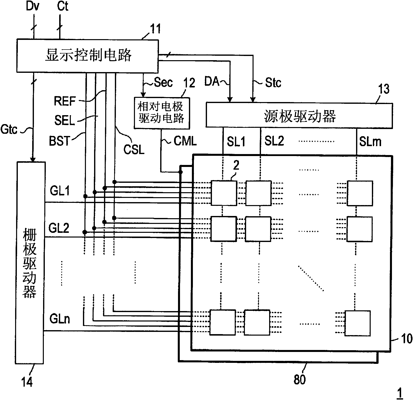
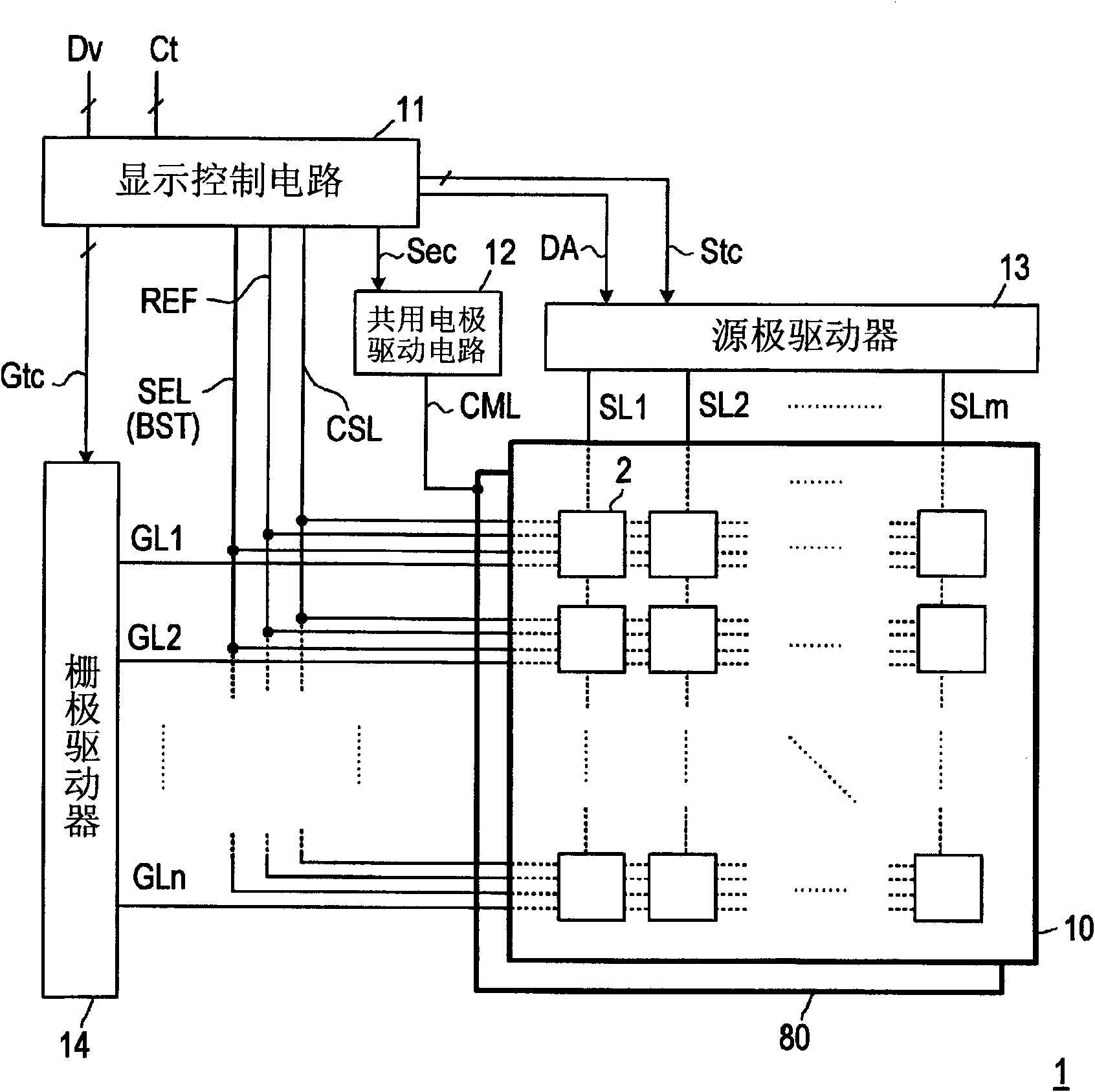
[0186] figure 1 A schematic configuration of the display device 1 is shown. The display device 1 includes an active matrix substrate 10 , counter electrodes 80 , a display control circuit 11 , a counter electrode drive circuit 12 , a source driver 13 , a gate driver 14 , and various signal lines described later. On the active matrix substrate 10, a plurality of pixel circuits 2 are respectively arranged in row and column directions, forming a pixel circuit array.
[0187] In addition, in figure 1 In , the pixel circuit 2 is displayed in blocks in order to avoid the complexity of the drawing. In addition, in order to clarify that various signal lines are formed on the active matrix substrate 10 , the a...
no. 2 Embodiment approach
[0239] In the second embodiment, circuits representing the first to sixth types described above will be described with reference to the drawings. Figure 6 The self-refresh operation of the first type pixel circuit 2A is shown. In addition, as will be described later, in other types of pixel circuits, a self-refresh operation can be realized similarly to the case of the first type.
[0240] The so-called self-refresh operation refers to the operation in the constant display mode to make the first switch circuit 22, the second switch circuit 23 and the control circuit 24 operate in a predetermined order for a plurality of pixel circuits 2, so that the potential of the pixel electrode 20 (This is also the potential of the internal node N1.) Simultaneously restores to the potential written in the immediately preceding write operation. The self-refresh operation is an operation unique to the present invention performed by the above-mentioned pixel circuits 2A to 2F. Compared with...
no. 3 Embodiment approach
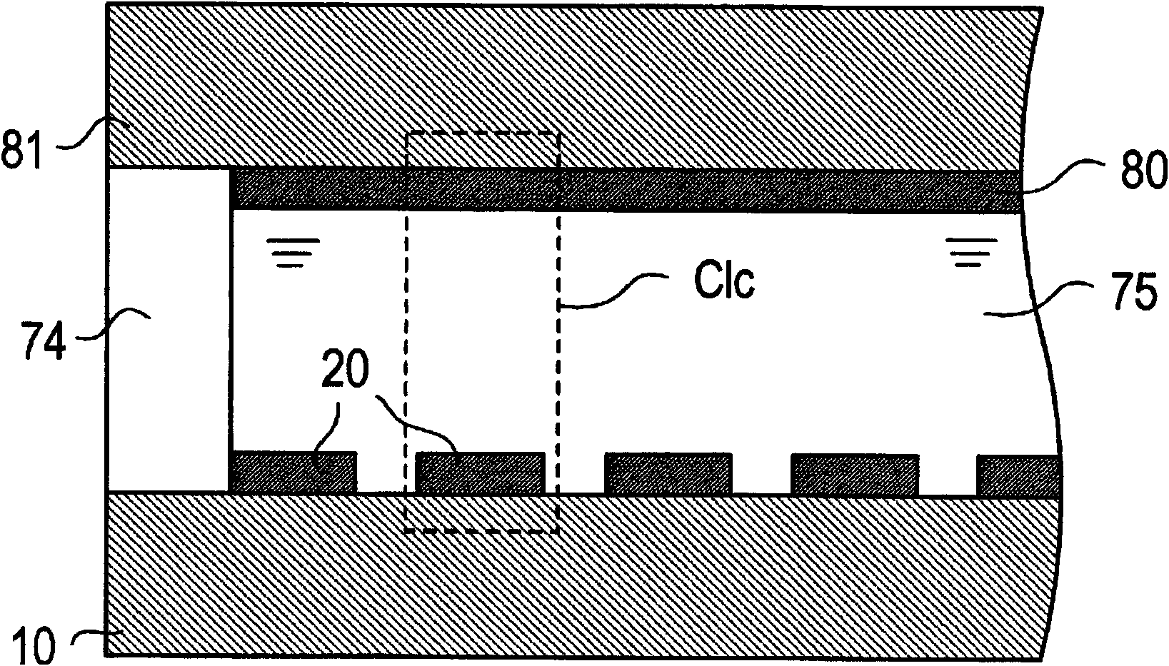
[0289] In the third embodiment, circuits representing the first to sixth types described above will be described with reference to the drawings. Figure 6 The self-polarity inversion operation of the first type pixel circuit 2A is shown. In addition, as will be described later, in other types of pixel circuits, the self-polarity inversion operation can be realized similarly to the case of the first type.
[0290] The so-called self-polarity inversion operation refers to an operation in which the first switch circuit 22, the second switch circuit 23, and the control circuit 24 are operated in a predetermined order for a plurality of pixel circuits 2 during the operation in the constant display mode, and the The polarity of the liquid crystal voltage Vlc applied between the pixel electrode 20 and the opposite electrode 80 is reversed altogether while maintaining its absolute value as it is. The self-polarity inversion operation is an operation unique to the present invention pe...
PUM
 Abstract
Description
Claims
Application Information
 - R&D
- Intellectual Property
- Life Sciences
- Materials
- Tech Scout
- Unparalleled Data Quality
- Higher Quality Content
- 60% Fewer Hallucinations
Browse by: Latest US Patents, China's latest patents, Technical Efficacy Thesaurus, Application Domain, Technology Topic, Popular Technical Reports.
© 2025 PatSnap. All rights reserved.Legal|Privacy policy|Modern Slavery Act Transparency Statement|Sitemap|About US| Contact US: help@patsnap.com