Liquid crystal display panel and repairing method of liquid crystal display panel

A liquid crystal display panel and repair method technology, applied in nonlinear optics, instruments, optics, etc., can solve problems such as inapplicability of repair methods and inability to completely repair bright spot defects, and achieve the effect of improving display quality

Active Publication Date: 2012-10-17
TCL CHINA STAR OPTOELECTRONICS TECH CO LTD
View PDF6 Cites 27 Cited by
  • Summary
  • Abstract
  • Description
  • Claims
  • Application Information

AI Technical Summary

Problems solved by technology

[0004] However, the above-mentioned existing repair methods can only repair bright spots into dark spots, and cannot completely repair bright spot defects; and, for panels with special electrode structure designs, such as display panels with electrode designs that do not require storage capacitors, existing repair methods method does not apply

Method used


Image

  • Liquid crystal display panel and repairing method of liquid crystal display panel
  • Liquid crystal display panel and repairing method of liquid crystal display panel
  • Liquid crystal display panel and repairing method of liquid crystal display panel

Examples


Embodiment Construction

[0021] The present invention will be described in detail below in conjunction with the accompanying drawings and embodiments.

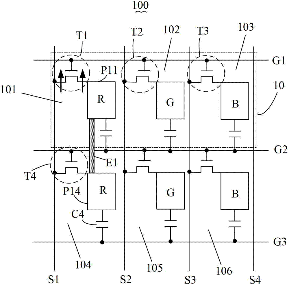
[0022] Please refer to figure 1 , figure 1 It is a partial structural schematic diagram of the first embodiment of a liquid crystal display panel of the present invention, as figure 1 As shown, the liquid crystal display panel 100 of the present invention includes a plurality of data lines, such as figure 1 S1, S2, S3, and S4 in S1, multiple scanning lines intersecting multiple data lines, such as figure 1 G1, G2 and G3 shown, and multiple sub-pixel regions, such as figure 1 101-106 shown.

[0023] In this embodiment, two adjacent data lines and two adjacent scan lines define a sub-pixel area, for example, the sub-pixel area 101 formed by intersections of the data lines S1 and S2 and the scan lines G1 and G2 respectively.

[0024] Since the structure of each sub-pixel area is the same, only the structure of the sub-pixel area 104 is exemplified b...


PUM


Abstract

The invention discloses a liquid crystal display panel and a repairing method of the liquid crystal display panel. The liquid crystal display panel comprises a plurality of data lines and a plurality of sub-pixel regions; each sub-pixel region comprises a corresponding pixel electrode and a thin-film transistor, wherein the sub-pixel region, in which a point defect exists, is electrically connected with a normal display sub-pixel region adjacent to the sub-pixel region; the sub-pixel region in which the point defect exists and the normal display sub-pixel region are used for displaying the same color; the connection among the thin-film transistor corresponding to the point defect, the corresponding data line and the pixel electrode is interrupted. In this way, the liquid crystal display panel and the repairing method can change a light spot to be a good spot so as to improve the display quality of the liquid crystal display panel, and the liquid crystal display panel can be suitable for repairing the liquid crystal display panel designed for the electrode not needing a storage capacitance.

Description

technical field [0001] The invention relates to the field of display technology, in particular to a liquid crystal display panel and a repair method thereof. Background technique [0002] At present, due to the process defects of TFT (Thin Film Transistor, Thin Film Field Effect Transistor), the internal electrical characteristics of individual TFTs will be abnormal, which will lead to point defects such as bright spots on the liquid crystal display panel, which will affect the display quality. [0003] For liquid crystal display panels, bright spots are a kind of point defects that are very difficult to solve. At present, the main solution is to use repairing methods to turn bright spots into dark spots. Among them, taking the vertical alignment (Vertical Alignment, VA) type display panel as an example, it is mainly to short-circuit the pixel electrode corresponding to the sub-pixel area where the bright spot appears and the common electrode of the storage capacitor, so tha...

Claims


Application Information

Patent Timeline
Patent Type & Authority Applications(China)
IPC IPC(8): G02F1/1362G02F1/1368G02F1/13
CPCG02F1/13G02F1/1362G02F1/1368G02F1/136259G02F1/136268
Inventor 刘涛叶冬徐亮严佩坚阙祥灯
Owner TCL CHINA STAR OPTOELECTRONICS TECH CO LTD
Why Eureka
Try Eureka