Temperature sensor as flip chip on a printed circuit board
A temperature sensor and circuit board technology, which is applied to thermometers, thermometers, instruments, etc. that use electric/magnetic components that are directly sensitive to heat, can solve problems such as unfavorable response time and variable measurement accuracy
- Summary
- Abstract
- Description
- Claims
- Application Information
AI Technical Summary
Problems solved by technology
Method used
Image
Examples
Embodiment 1
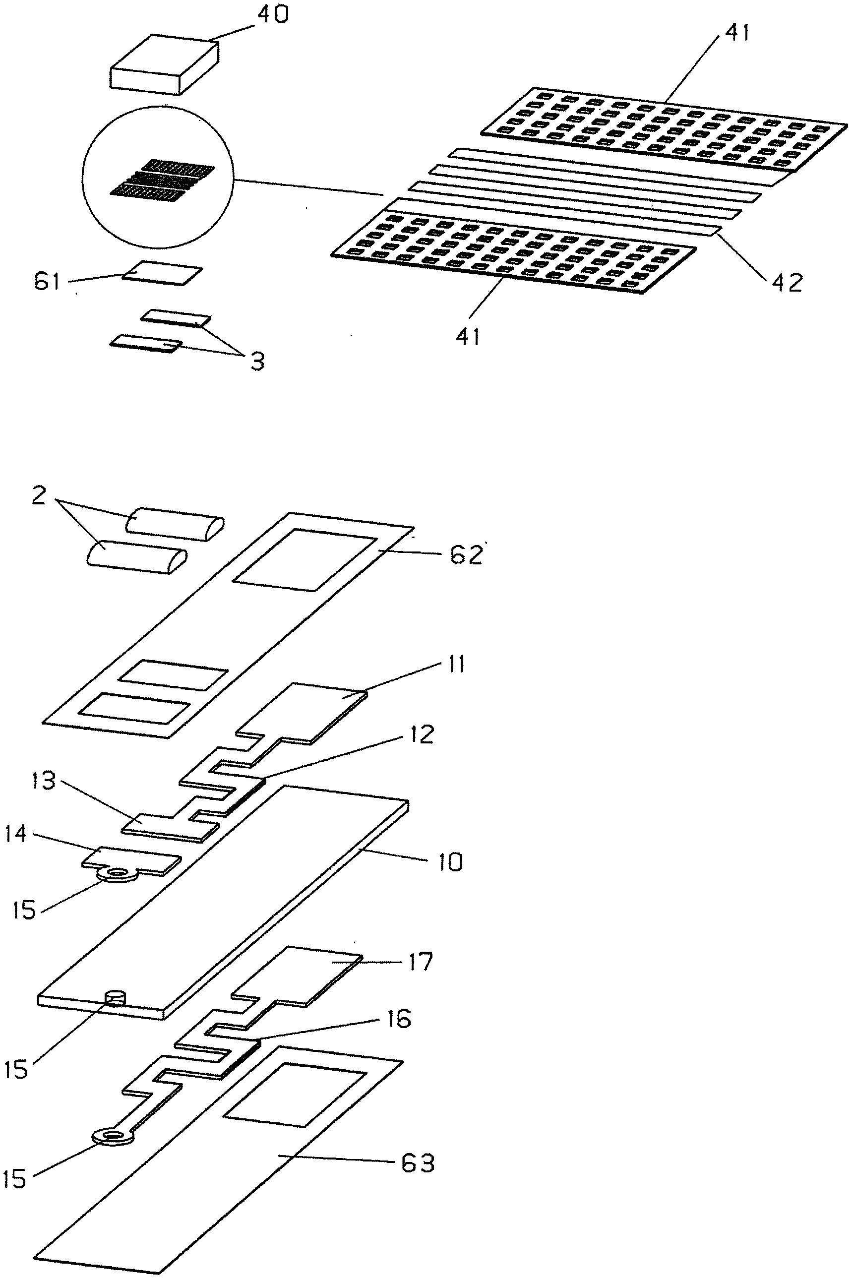
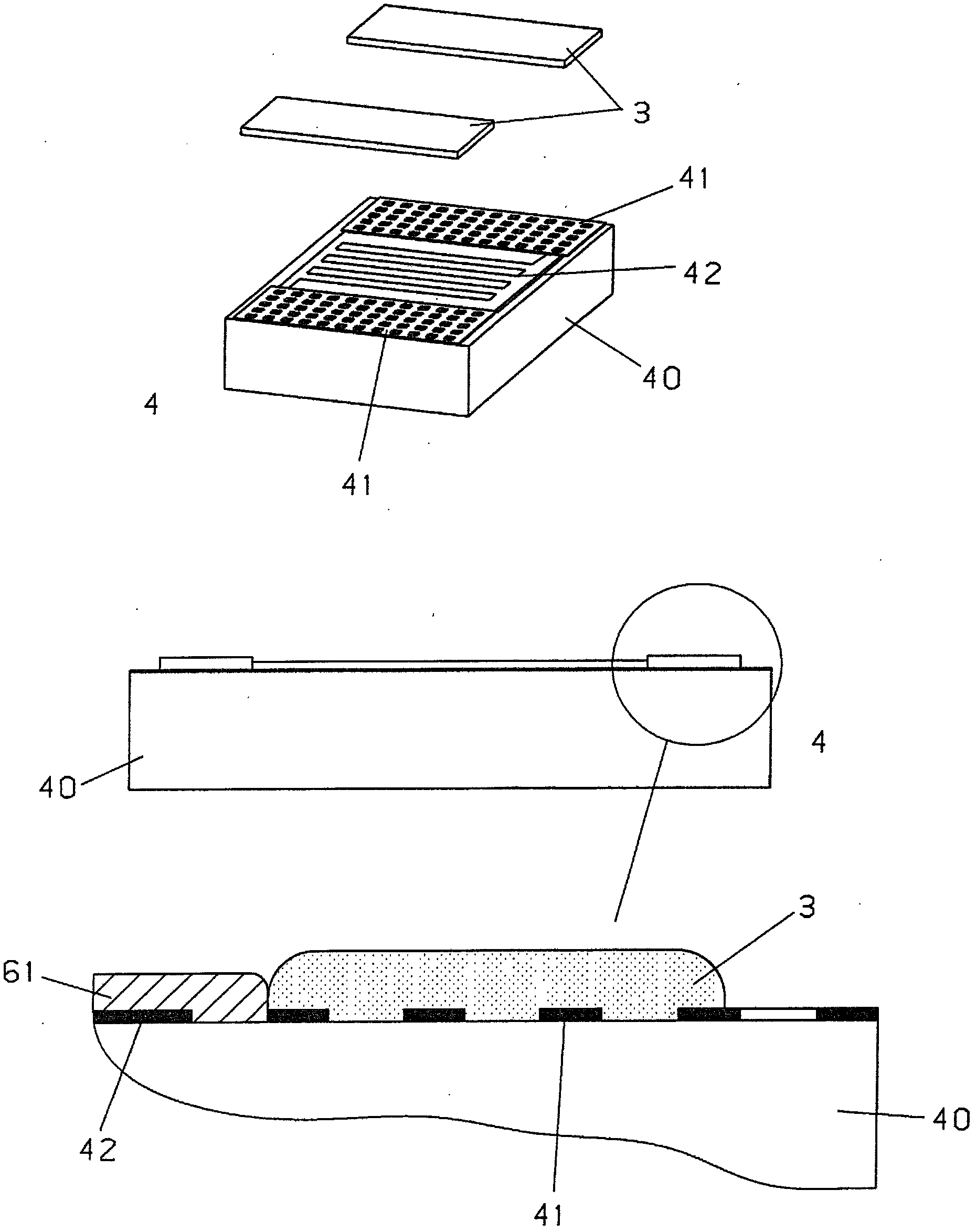
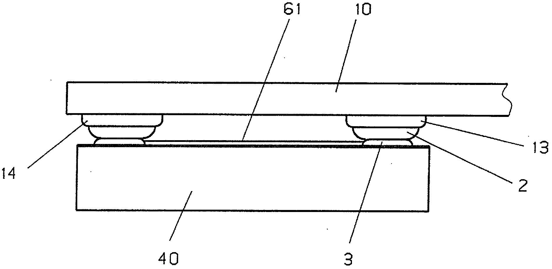
[0056] A piece of 300 mm x 150 mm x 0.4 mm BT epoxy resin foil 10 plated with 50 μm copper on both sides and reinforced with glass fibers was processed into 1000 larger units 1 of 15 mm x 3 mm. Here, each unit 1 is provided with a contact spread 15 at one end and with a larger contact area 11, 17 of 3.5 x 2.5 mm on the front and back at the other end. The larger contact area 11 is connected to the smaller contact area 13 via a guide rail 12 in a meandering manner. On the opposite side, the contact expansion 15 is connected to the larger contact area 17 via meander-shaped guide rails 16 . Two smaller contact areas 13 , 14 of 1.5 mm extending in the longitudinal direction of the printed circuit board 1 are provided on the front side and are bridged by the flip chip 4 . The contact extension 15 is arranged on one of the smaller contact areas 14 .
[0057] The contact area is plated with soft solder 2. The soft solder 2, in particular the smaller contact areas 13, 14, contains ...
Embodiment 2
[0063] A piece of 150 mm x 100 mm x 0.3 mm BT epoxy resin foil coated with 50 μm copper on both sides and reinforced with glass fibers was processed into 500 smaller units 1 , in particular with dimensions of 10 mm x 2.5 mm. Here, each unit 1 is provided with a contact spread 15 at one end and with a larger contact area 11 , 17 of 2.5×2 mm on the front and back at the other end. On the opposite side, the contact extension 15 is connected to the contact area 17 via the guide rail 16 . Two smaller contact areas 13 , 14 of 1 mm extending in the longitudinal direction of the printed circuit board 1 are provided on the front side and are bridged by the flip chip 4 . During the processing of the copper coating, the smaller contact area 13 in this area is connected to the larger contact area 11 via the guide rail 12 . The current spreader 15 is formed outside the small contact region 14 . A linear, 1 mm wide guide rail 16 is formed between the contact extension 15 and the larger co...
PUM
| Property | Measurement | Unit |
|---|---|---|
| electrical resistance | aaaaa | aaaaa |
Abstract
Description
Claims
Application Information


