Method for manufacturing semiconductor device
A semiconductor and chip technology, applied in the direction of semiconductor/solid-state device manufacturing, semiconductor devices, semiconductor/solid-state device components, etc., can solve the problems of reduced reliability and inability to distribute semiconductor chips evenly, and achieve uniform distribution in the plane
- Summary
- Abstract
- Description
- Claims
- Application Information
AI Technical Summary
Problems solved by technology
Method used
Image

Examples
Embodiment Construction
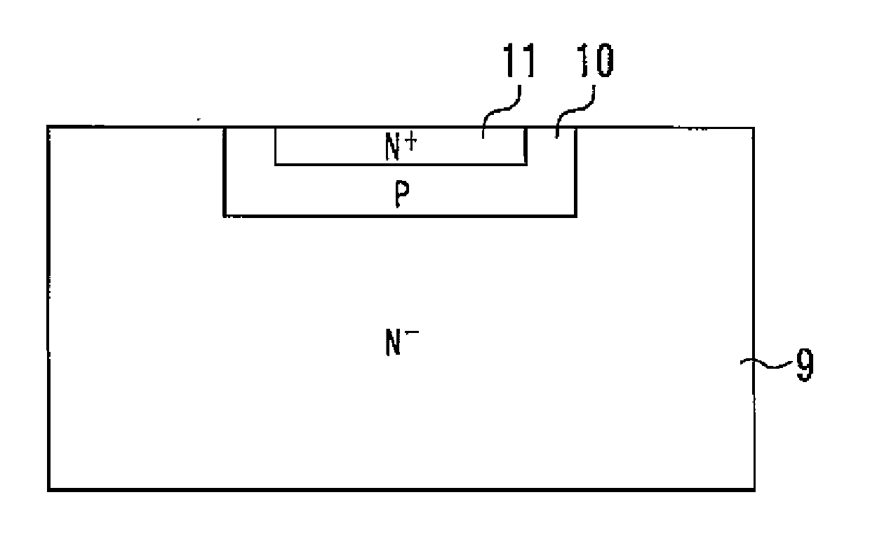
[0023] figure 1 It is a cross-sectional view showing a semiconductor device according to an embodiment of the present invention. The back surface of the semiconductor chip 1 is bonded to an electrode substrate 3 with a conductive bonding material 2 . The conductive bonding material 2 is solder, Ag paste, conductive adhesive, or the like. The electrode substrate 3 is mounted on a heat sink 5 via an insulating sheet 4 having excellent thermal conductivity. The surface of the semiconductor chip 1 is connected to external wiring terminals 7 by wires 6 such as Al or Cu. The semiconductor chip 1 , a part of the electrode substrate 3 , the insulating sheet 4 , a part of the heat sink 5 , the wire 6 , and a part of the external wiring terminal 7 are sealed with an insulating resin 8 .
[0024] Next, the manufacturing process of the semiconductor chip 1 will be described with reference to the drawings. Figure 2 to Figure 8 It is a sectional view showing the manufacturing process o...
PUM
 Abstract
Description
Claims
Application Information