Eureka AIR delivers breakthrough ideas for toughest innovation challenges, trusted by R&D personnel around the world.

Method for evaluating wafer and method for manufacturing epitaxial wafer

A technology for evaluating methods and manufacturing methods, applied in semiconductor/solid-state device manufacturing, electrical components, circuits, etc.

Pending Publication Date: 2019-01-15
SHIN-ETSU HANDOTAI CO LTD
View PDF4 Cites 0 Cited by
  • Summary
  • Abstract
  • Description
  • Claims
  • Application Information

AI Technical Summary

Problems solved by technology

[0003] Since the reaction raw materials are usually not actively provided on the inner surface of the wafer, a huge reaction like that on the outer surface does not take place on the inner surface of the wafer, but only a slight deposition reaction and an etching reaction coexist, resulting in Concave and convex parts related to the design of the base

Method used


Image

  • Method for evaluating wafer and method for manufacturing epitaxial wafer
  • Method for evaluating wafer and method for manufacturing epitaxial wafer
  • Method for evaluating wafer and method for manufacturing epitaxial wafer

Examples


Embodiment 1

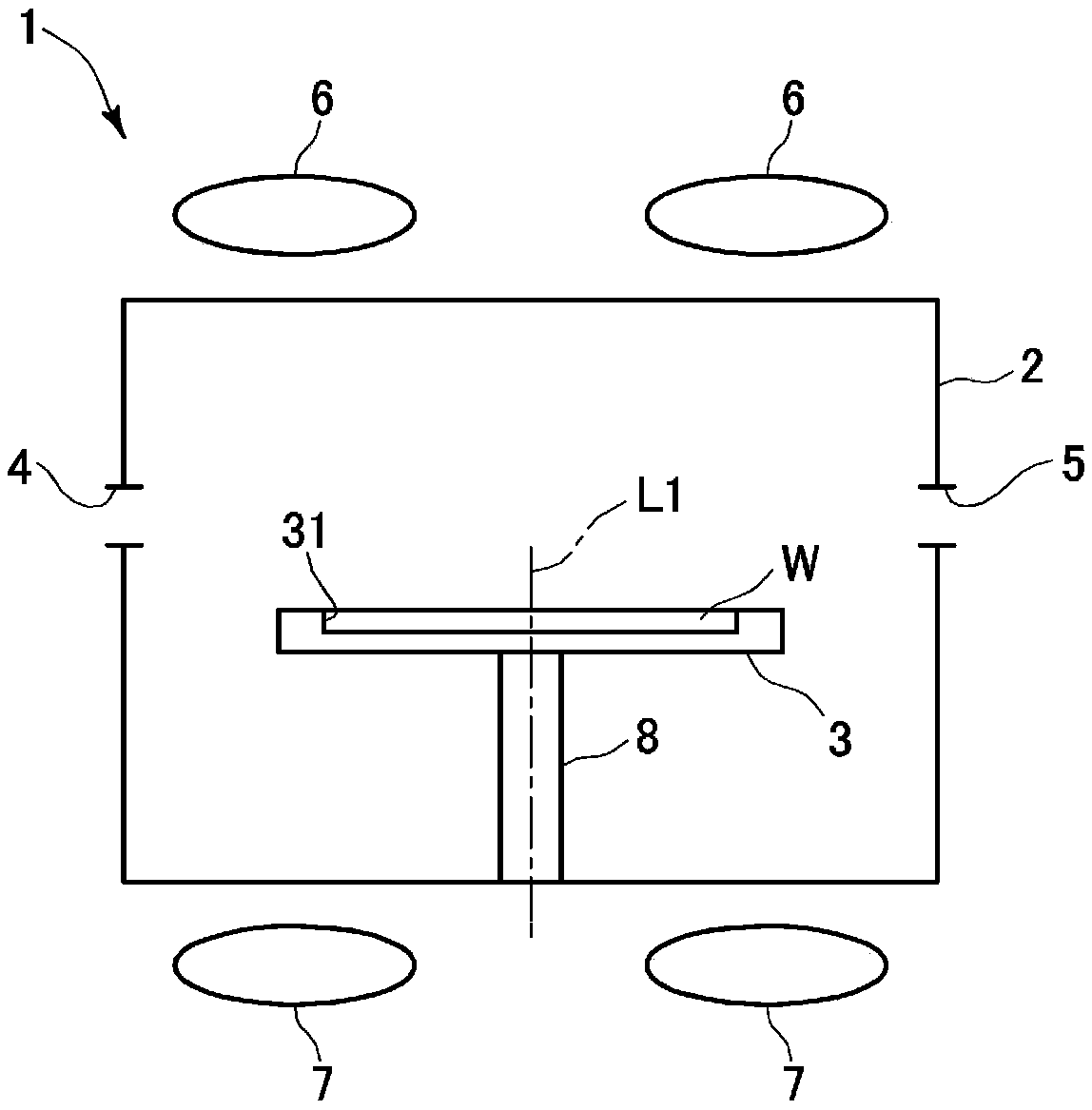
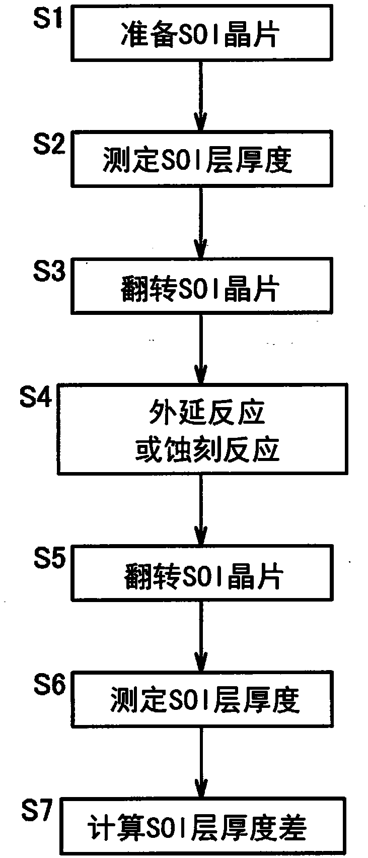
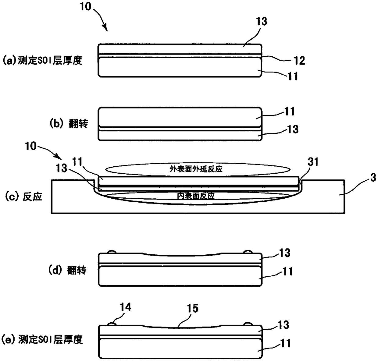
[0055] adopted with figure 1 The same epitaxial growth setup, according to figure 2 In the step of , the inner surface distribution of the deposited amount or the etched amount of the wafer inner surface (SOI layer) is obtained. At this time, in the step S4, the silicon source gas supplied to the SOI wafer is DCS (dichlorosilane) gas, so that the deposition reaction (epitaxy reaction) mainly proceeds on the outer surface of the silicon substrate of the SOI wafer. In addition, on multiple SOI wafers, one at a time figure 2 At this time, for different SOI wafers, the power ratios of the upper lamp and the upper lamp in the process of S4 are made different.

[0056] The in-plane distribution of the deposition amount or etching amount of the inner surface (SOI layer) of each SOI wafer is as follows: Figure 4 shown. Figure 4 It shows that the ratio of the power of the lower lamp to the total power of the upper lamp and the lower lamp is 47% (Lwr47), 51% (Lwr51), 55% (Lwr55)...

Embodiment 2

[0061] adopted with figure 1 The same epitaxial growth setup, according to figure 2 The in-plane distribution of the amount of deposition or etching on the inner surface of the wafer (SOI layer) is obtained. At this time, in the step S4, HCl gas is supplied to the outer surface of the SOI wafer, so that the etching reaction mainly proceeds on the outer surface of the silicon substrate of the SOI wafer. Reaction conditions (flow rate of HCl gas, etc.) were set such that the etching amount of the outer surface of the silicon substrate was 0.5 μm. In addition, a base having a plurality of dimples on the bottom surface of the base recess is prepared. Next, using this susceptor, HCl gas is supplied to the outer surface of the SOI wafer to cause a reaction.

[0062] When HCl gas is supplied to the outer surface of the SOI wafer, the in-plane distribution of the deposition amount or the etching amount of the inner surface (SOI layer) of the SOI wafer is as follows: Figure 5 , ...


PUM


Abstract

A method is provided which is capable of determining which of the deposition reaction and the etching reaction is causing wafer inner surface concave-convex portions with respect to the epitaxial reaction or the etching reaction on the outer surface of the wafer. A SOI wafer (S1) is prepared, and the thickness (S2) of the SOI layer of the SOI wafer was measured. The SOI wafer is turned upside downand placed on a pedestal so that the SOI layer faces the pedestal side, and the epitaxial reaction or the etching reaction (S3, S4) are performed. The SOI wafer after the reaction is inverted upsidedown so that the SOI layer is directed upward, and the thickness (S5, S6)of the SOI layer is measured. The in-plane distribution (S7) of the deposition reaction and the etching reaction on the inner surface of the wafer is obtained by determining the difference in thickness of the SOI layer before and after the reaction. Further, based on the obtained in-plane distribution, process conditions forepitaxial production for homogenizing the in-plane distribution are determined, and epitaxial growth is performed on the product substrate in accordance with the process conditions.

Description

technical field [0001] The present invention relates to a method of evaluating a reaction occurring on the inner surface of a wafer, which is accompanied by a deposition reaction (reaction of build-up deposition (film)) or an etching reaction on the outer surface of a wafer placed on a susceptor, and a method of manufacturing an epitaxial wafer And produced. Background technique [0002] With the high integration of semiconductor devices, the requirements for the quality of wafers constituting their raw materials have further increased. For epitaxial wafers, in addition to the flattening of the film thickness distribution of the epitaxial layer vapor grown on the outer surface, the smoothing of the unevenness of the inner surface (the wafer surface opposite to the side where the epitaxial layer is formed) is also a smoothness quality. One of the improved items. [0003] Since the reaction raw materials are usually not actively provided on the inner surface of the wafer, a ...

Claims


Application Information

Patent Timeline
IPC IPC(8): H01L21/66
CPCH01L22/12H01L22/20H01L21/31116
Inventor 大西理荒井刚
Owner SHIN-ETSU HANDOTAI CO LTD
Why Eureka
Eureka Blog
Learn More