Method of manufacturing an x-ray diffraction grating microstructure for imaging apparatus

A manufacturing method and microstructure technology, applied in the application of diffraction/refraction/reflection for processing, imaging devices, semiconductor/solid-state device manufacturing, etc., and can solve problems such as microstructures that are not discussed

Inactive Publication Date: 2012-12-05
CANON KK
View PDF6 Cites 10 Cited by
  • Summary
  • Abstract
  • Description
  • Claims
  • Application Information

AI Technical Summary

Problems solved by technology

[0005] However, PTL 1 does not discuss methods for

Method used


Image

  • Method of manufacturing an x-ray diffraction grating microstructure for imaging apparatus
  • Method of manufacturing an x-ray diffraction grating microstructure for imaging apparatus
  • Method of manufacturing an x-ray diffraction grating microstructure for imaging apparatus

Examples


Embodiment Construction

[0020] Various exemplary embodiments, features, and aspects of the present invention will be described in detail below with reference to the accompanying drawings.

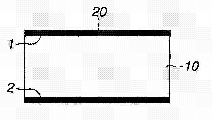
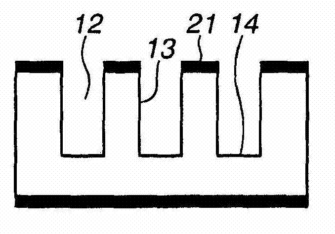
[0021] FIG. 1 shows a first exemplary embodiment of a microstructure manufacturing method according to the present invention. The manufacturing method is a method including forming a microstructure on one surface of a Si substrate and forming a metal microstructure by applying electrolytic plating to the inside of the Si microstructure while using the Si microstructure as a mold.

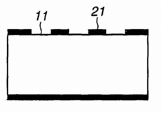
[0022] First, a first insulating film is formed on the front and back surfaces of the Si substrate (first process). Such as Figure 1A As shown in , a first insulating film 20 is formed on the front side 1 and the back side 2 of the Si substrate 10 . The size and thickness of the Si substrate 10 may be determined according to a desired microstructure. In addition, the resistivity of Si substrate 10 is 10 Ωcm or less, preferably or op...


PUM


Abstract

A microstructure manufacturing method includes forming a first insulating film on an Si substrate, exposing an Si surface by removing a part of the first insulating film, forming a recessed portion by etching the Si substrate from the exposed Si surface, forming a second insulating film on a sidewall and a bottom of the recessed portion, forming an Si exposed surface by removing at least a part of the second insulating film formed on the bottom of the recessed portion, and filling the recessed portion with a metal from the Si exposed surface by electrolytic plating.

Description

technical field [0001] The present invention relates to a method for producing microstructures, and in particular to a method for producing microstructures, in particular microstructures with high aspect ratios, by electrolytic plating of metal with a mold. Background technique [0002] Micro-fine structures with periodic structures (especially high-aspect-ratio structures) are required in many fields. For example, the X-ray absorption properties of microstructures composed of gold are used in non-destructive testing of objects as industrial applications and also in radiography, for example as medical applications. Microstructures in these applications form contrast images by utilizing density variations according to objects or biological objects and absorption differences upon X-ray transmission of constituent elements, and are called X-ray absorption contrast methods. [0003] In addition, since even light elements can be imaged by the phase contrast method using the phas...

Claims


Application Information

Patent Timeline
IPC IPC(8): C25D5/02C25D7/00C25D7/12G21K1/06H01L21/768
CPCC25D5/022G21K2207/005C25D7/00H01L21/76877C25D7/123C25D7/12G21K1/06G21K1/02
Inventor 王诗男中村高士手岛隆行濑户本丰渡边信一郎
Owner CANON KK
Why Eureka
Try Eureka