Touch screen, touch display device and production method of touch screen

A manufacturing method and touch screen technology are applied in the field of touch screen manufacturing, touch screen and touch display device, and can solve the problems of affecting the display effect of the touch display device and reducing the light transmittance of the touch screen, so as to improve the macro color effect and improve the light The effect of reducing transmittance and coverage area

Inactive Publication Date: 2012-12-19
BEIJING BOE OPTOELECTRONCIS TECH CO LTD
View PDF4 Cites 11 Cited by
  • Summary
  • Abstract
  • Description
  • Claims
  • Application Information

AI Technical Summary

Problems solved by technology

[0011] The invention provides a touch screen, a touch display device and a manufacturing method of the touch screen, which are used to solve the problem that the light transmittance of the touch screen is greatly reduced due to the existence of a large insulating layer in the prior art, thereby affecting the touch display device. Technical problems with the display effect

Method used


Image

  • Touch screen, touch display device and production method of touch screen
  • Touch screen, touch display device and production method of touch screen
  • Touch screen, touch display device and production method of touch screen

Examples


Embodiment Construction

[0046] In order to solve the technical problem that the insulating layer exists in a large area in the prior art, which greatly reduces the light transmittance of the touch screen and affects the display effect of the touch display device, the present invention provides a touch screen, a touch display device and a touch screen manufacturing method.

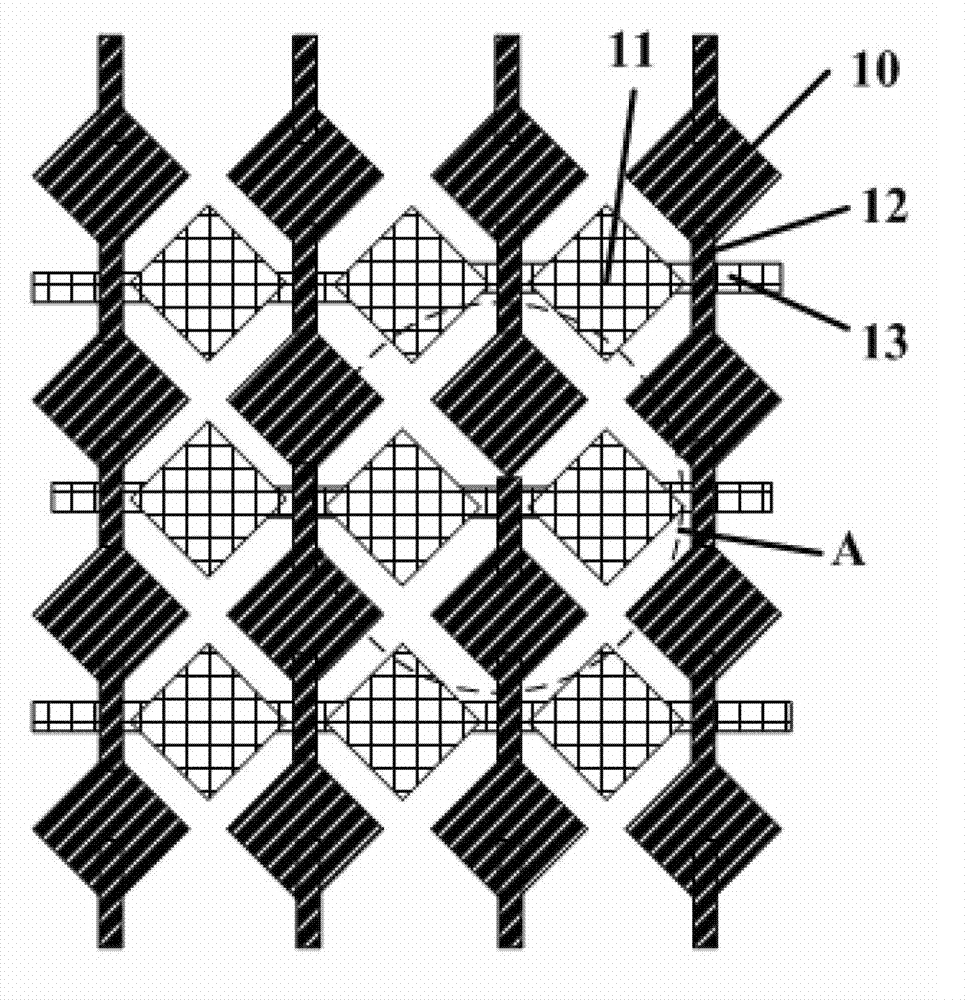
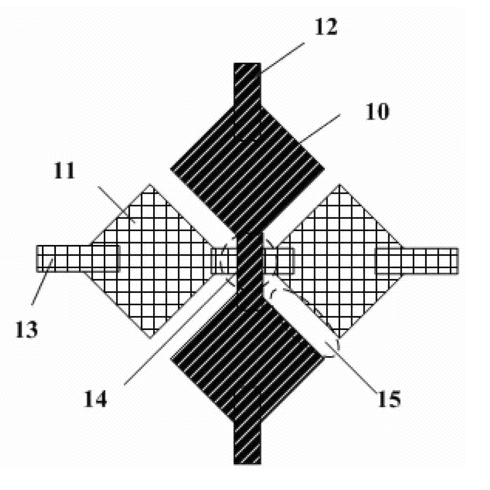
[0047] Such as image 3 As shown, the touch screen of the present invention includes on the transparent substrate:

[0048] The first electrode 10, the second electrode 11 and the second electrode connection line 13 on the first layer, the first electrode 10 and the second electrode 11 are arranged in a cross, and the second electrode connection line 13 connects Adjacent second electrodes 11 are connected;

[0049] The first electrode connecting wire 12 on the second layer overlaps the adjacent first electrodes 10 at the intersection;

[0050] An insulating block 160 located between the first electrode connecting line 12 and th...


PUM


Abstract

The invention discloses a touch screen, a touch display device and a production method of the touch screen. The touch screen comprises first electrodes, second electrodes, second electrode connecting wires, first electrode connecting wires, insulating blocks and a protective layer. The first electrodes, the second electrodes and the second electrode connecting wires are arranged on a first level. The first electrodes and the second electrodes intersect with each other. The second electrode connecting wires connect the adjacent second electrodes at the intersection. The first electrode connecting wires on a second level connect the adjacent first electrodes at the intersection in an overlapping manner. The insulating blocks located between the first electrode connecting wires and the second electrode connecting wires are overlapped with the first electrode connecting wires. The arrangement size of the insulating blocks in the direction of the first electrodes is smaller than the length of each first electrode connecting wire, and the arrangement size of the insulating block in the direction of the second electrodes is not smaller than the width of each first electrode connecting wire. The protective layer is arranged above the structure of the first level, the insulating blocks and the second level. Light transmissivity of the touch screen is improved greatly, macroscopic color effect is improved, and touch resistance between the first electrodes is also reduced.

Description

technical field [0001] The present invention relates to the technical field of touch display, in particular to a touch screen, a touch display device and a manufacturing method of the touch screen. Background technique [0002] As an input medium, a touch screen provides users with better convenience than a keyboard and a mouse. According to different implementation principles, touch screens can be divided into resistive, capacitive, surface acoustic wave, infrared, bending wave, active digital converter, and optical imaging. At present, resistive and capacitive touch screen technologies are widely used. In the structures of these two touch screens, transparent metal electrodes need to be provided. [0003] Compared with resistive touch screens, capacitive touch screens have the advantages of fast response time, good reliability and high durability. Capacitive touch screens include surface capacitive and inductive capacitive, and inductive capacitive touch screens can be d...

Claims


Application Information

Patent Timeline
Patent Type & Authority Applications(China)
IPC IPC(8): G06F3/041
Inventor 曲连杰郭建王智勇阎长江
Owner BEIJING BOE OPTOELECTRONCIS TECH CO LTD
Why Eureka
Try Eureka