Semiconductor device and method of writing data to semiconductor device

A data writing, semiconductor technology, applied in the direction of secure communication devices, digital transmission systems, response error generation, etc., can solve the problems of not being able to fully improve the security of semiconductor devices, and achieve security improvement and high security communication Effect

Active Publication Date: 2012-12-26
RENESAS ELECTRONICS CORP
View PDF10 Cites 16 Cited by
  • Summary
  • Abstract
  • Description
  • Claims
  • Application Information

AI Technical Summary

Problems solved by technology

Therefore, there is a problem that even when the techniques disclosed in Patent Documents 1 to 4 are applied, the security of the semiconductor device cannot be sufficiently improved

Method used


Image

  • Semiconductor device and method of writing data to semiconductor device
  • Semiconductor device and method of writing data to semiconductor device
  • Semiconductor device and method of writing data to semiconductor device

Examples


no. 1 example

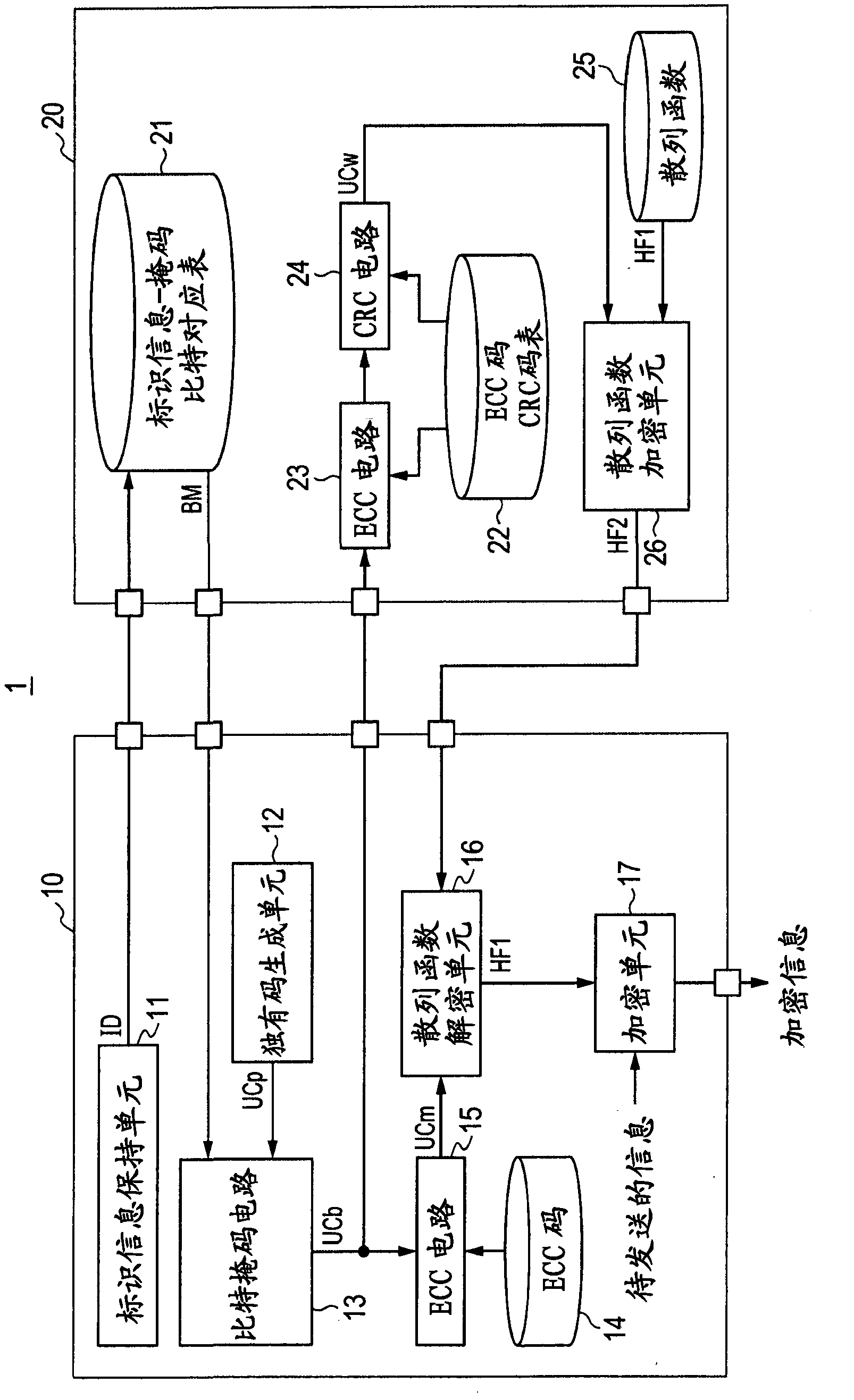
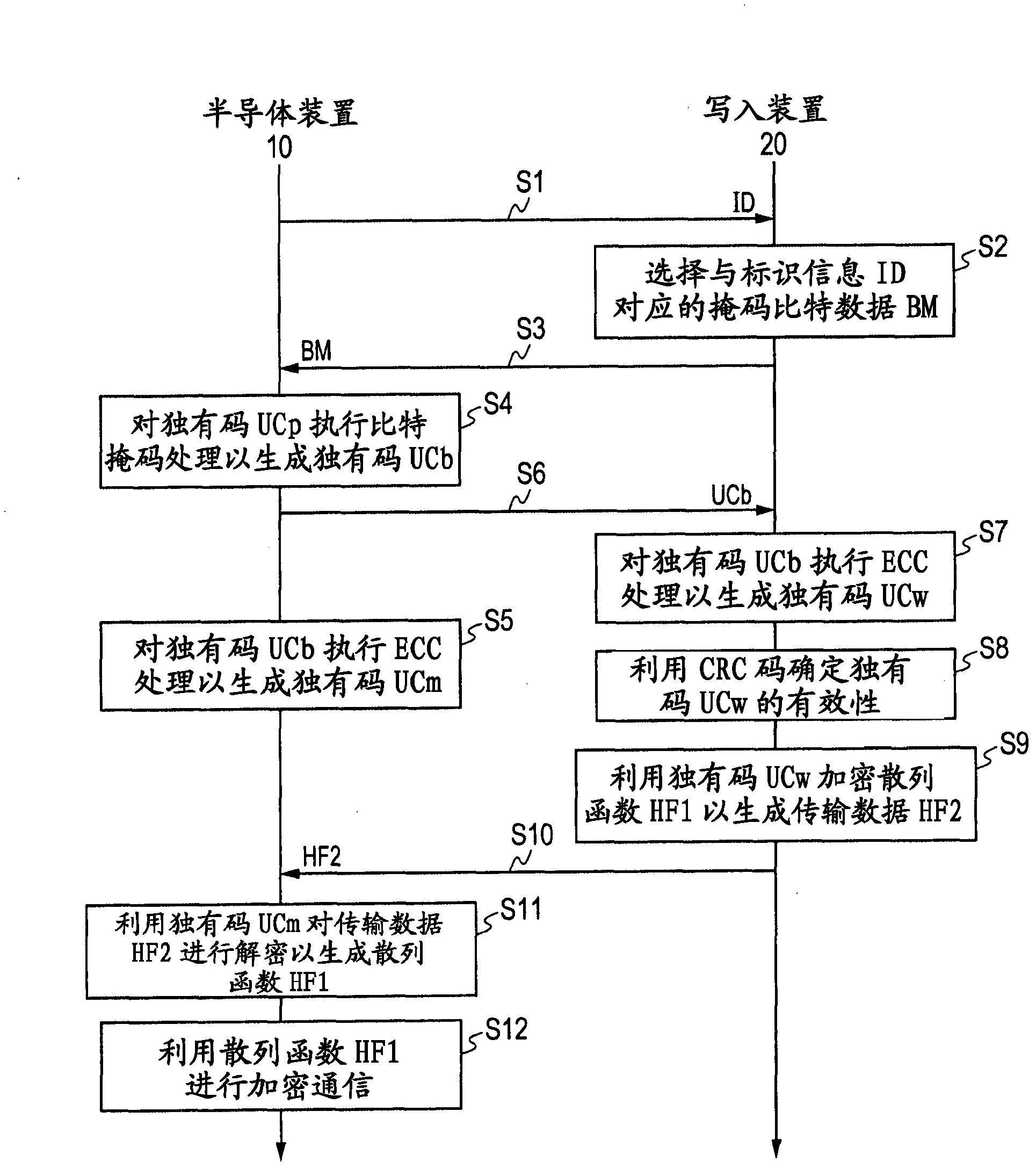
[0038] Embodiments of the present invention will be described below with reference to the drawings. figure 1 is a block diagram showing the semiconductor device 10 according to the first embodiment and an external device (for example, the writing device 20 ). Such as figure 1 As shown in , in the first embodiment, the semiconductor device 10 and the external device 20 configure one data writing system 1 . In the semiconductor device 10, confidential information is written by the data writing system 1, and encrypted communication is performed using the confidential information.

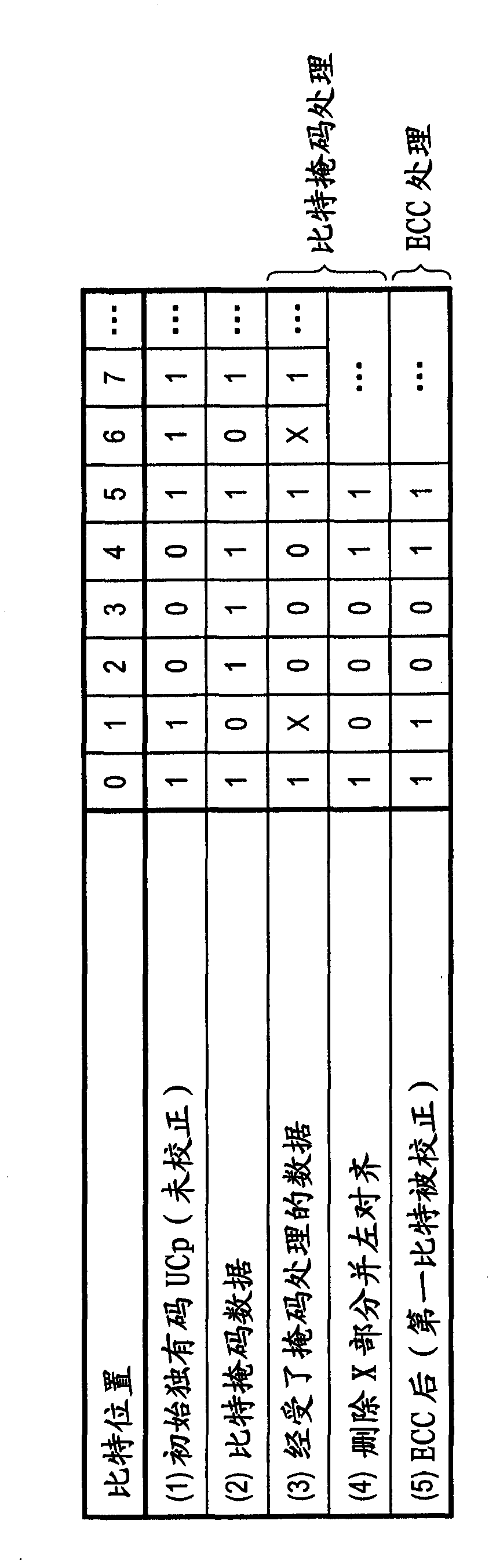
[0039] Such as figure 1 As shown in , the semiconductor device 10 has a unique code generation unit 12, a first error correction unit (for example, a bit mask circuit 13), a second error correction unit (for example, an ECC circuit 15), and a decryption unit (for example, a decryption column function decryption unit 16). The semiconductor device 10 also has an identification information holding uni...

no. 2 example

[0079] Figure 4 is a block diagram of the semiconductor device 30 and an external device (for example, the writing device 40 ) according to the second embodiment. Such as Figure 4 As shown in , in the second embodiment, the data writing system 2 is configured by a semiconductor device 30 and a writing device 40 . In the description of the second embodiment, the same reference numerals as in the first embodiment are assigned to the same components as in the first embodiment, and description thereof will not be repeated.

[0080] Such as Figure 4 As shown in , a semiconductor device 30 has an ECC circuit 31 as a first data correction unit in the semiconductor device 10 according to the first embodiment and a bit mask circuit 33 as a second data correction unit. In the semiconductor device 30, the bit mask data BM is used as the second correction data used in the second data correction unit. exist Figure 4 In , the storage unit 32 is shown as an area for storing the bit ...

no. 3 example

[0091] Figure 6 is a block diagram of a semiconductor device 50 and an external device (for example, a writing device 60 ) according to the third embodiment. Such as Figure 6 As shown in , in the third embodiment, a data writing system 3 is configured by a semiconductor device 50 and a writing device 60 . In the description of the third embodiment, the same reference numerals as in the first embodiment are assigned to the same components as in the first embodiment, and description thereof will not be repeated.

[0092] Such as Figure 6 As shown in , according to the third embodiment, the semiconductor device 60 maintains an identification-bit mask correspondence table in an encrypted state. exist Figure 6 In , the area with the encrypted identification information-bit mask correspondence table is shown as the storage unit 61 . In the case of receiving the identification information ID, the storage unit 61 outputs the bit mask data BME subjected to encryption processin...


PUM


Abstract

The invention relates to a semiconductor device and a method of writing data to a semiconductor device. The semiconductor device in related art has a problem that security at the time of writing data cannot be sufficiently assured. A semiconductor device of the present invention has: a unique code generating unit generating an initial unique code which is a value unique to a device and includes an error in a random bit; a first error correcting unit correcting an error in the initial unique code to generate an intermediate unique code; a second error correcting unit correcting an error in the intermediate unique code to generate a first determinate unique code; and a decrypting unit decrypting, with the first determinate unique code, transmission data obtained by encrypting confidential information with key information generated on the basis of the intermediate unique code by an external device to generate confidential information.

Description

[0001] Cross References to Related Applications [0002] The disclosure of Japanese Patent Application No. 2011-136133 filed on Jun. 20, 2011 including application documents, drawings and abstract is incorporated herein by reference in its entirety. technical field [0003] The present invention relates to a semiconductor device and a method of writing data to the semiconductor device, and more particularly, to a semiconductor device that holds secret information to keep it secret from an attack from the outside, and to a method of writing secret information to the semiconductor device method. Background technique [0004] In recent years, many security technologies for improving resistance to unauthorized access of semiconductor devices or preventing counterfeiting using encryption technology have been proposed. In the encryption technique, an encryption key is used. However, this technique has a problem that when an attacker obtains an encryption key, illegal access to t...

Claims


Application Information

Patent Timeline
Patent Type & Authority Applications(China)
IPC IPC(8): H04L9/32
CPCH04L9/3278H04L2209/04H04L2209/34H04L2209/08G06F11/10G11C7/24G11C29/42H03M13/29H03M13/63H04L9/3226
Inventor 押田大介古田茂广川祐之山崎晓藤森隆盐田茂雅
Owner RENESAS ELECTRONICS CORP
Why Eureka
Try Eureka