Light emitting device

A technology for light-emitting devices and light-emitting elements, which is applied to electrical components, electrical solid-state devices, circuits, etc., can solve problems such as hindering heat dissipation, uneven stress distribution, and thermal deviation in light-emitting devices, and achieves high reliability and improved heat dissipation. , to prevent the effect of uneven distribution

Inactive Publication Date: 2013-01-02
TOYODA GOSEI CO LTD
View PDF6 Cites 1 Cited by
  • Summary
  • Abstract
  • Description
  • Claims
  • Application Information

AI Technical Summary

Problems solved by technology

[0007] However, the invention described in Patent Reference 1 has the problem that since the size and shape of each individual lead frame and its arrangement are asymmetrical with respect to the case, heat is deviated in the light emitting device, thereby generating a local high temperature portion, and due to Thermal expansion applied to the shell, stress distribution becomes uneven
[0010] However, when the invention of Patent Reference 2 is employed in a side-view type light emitting device, in order to dissipate the heat of the base arranged at the center to the outside, it is necessary to extend the suspension leads or other dedicated heat radiation protruding to the outside. The lead frame is connected to the base, but the lead frame dedicated to heat dissipation protruding to the outside hinders the attempt to form a thinner and smaller light emitting device, which is not desirable
[0011] In addition, since a plurality of light emitting elements are mounted on the base arranged at the center, the heat dissipation path cannot be divided and heat dissipation is hindered, which is also undesirable.

Method used


Image

  • Light emitting device
  • Light emitting device
  • Light emitting device

Examples


Embodiment approach 1

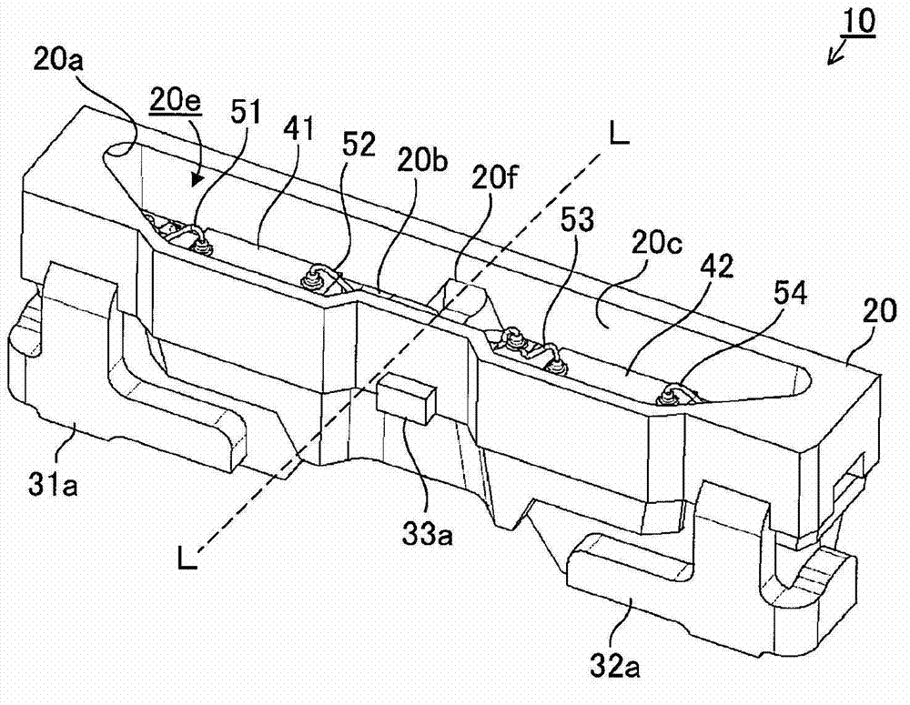
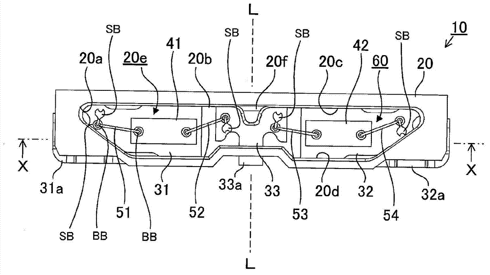
[0049] As shown in FIGS. 1 and 2 , the light-emitting device 10 in Embodiment 1 includes a housing 20 (including an opening 20 a , a bottom surface 20 b , inner surfaces 20 c , 20 d , an accommodation recess 20 e , and a columnar portion 20 f ), and a lead frame 31 . to 33, light emitting elements 41, 42, bonding wires 51 to 54, sealing resin 60, and the like. The light emitting device 10 is a side-view type light emitting device that emits light in a side surface direction (side surface light emitting device).

[0050] The light emitting device 10 has an elongated and flat shape. With respect to the center line (reference line) L that bisects the longitudinal direction, the members (housing 20, lead frames 31 to 33, and light emitting elements 41, 42) other than the bonding lines 51 to 54 are arranged and formed in a linear symmetrical configuration .

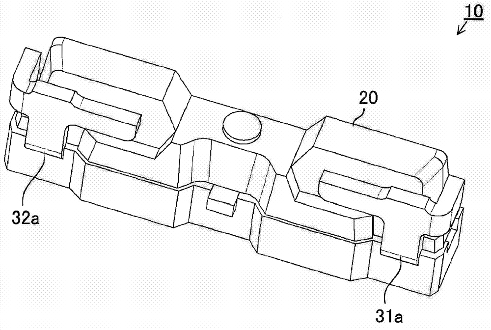
[0051] The housing (encapsulation portion) 20 has an elongated and flat box shape, and is integrally formed by synthetic r...

no. 2 approach )

[0097] As shown in FIG. 3 , the light-emitting device 100 of Embodiment 2 is a side-view type light-emitting device, which includes a case 20 (opening portion 20a, bottom surface 20b, inner side surfaces 20c, 20d, accommodating recessed portion 20e, and cylindrical portion 20f), lead frames 31 to 33, light emitting elements 41, 42, bonding wires 51 to 54, sealing resin 60, and the like.

Embodiment approach 2

[0098] The case 20 in Embodiment 2 is the same as the case 20 in Embodiment 1. As shown in FIG. Therefore, an oblique view of the light emitting device 100 is similar to the light emitting device 10 in Embodiment 1 as shown in FIG. 1 .

[0099] Embodiment 2 differs from Embodiment 1 in that the light emitting elements 41, 42 are not arranged in a linear asymmetric configuration with respect to the center line L, and the distance from the light emitting device 41 to the inner side surface 20c of the housing 20 is shorter than from the light emitting device 41 to the inner surface 20c of the casing 20. The distance from the device 42 to the inside surface 20c.

[0100]That is, in Embodiment 2, the light emitting device 41 is arranged in a region close to the inner side surface 20c of the case, and the light emitting device 42 is arranged in a region near the inner side surface 20c of the case.

[0101] In Embodiment 2, exactly as in Embodiment 1, the outer surfaces of the lead ...


PUM


Abstract

A light emitting device comprises two or more light emitting elements, two or more lead frames electrically connected to the light emitting elements, and a case formed as a slender flat box shape and having an accommodating recession for accommodating the light emitting elements and the lead frame, wherein the lead frames are buried in the case and provided side by side in a longitudinal direction of the case, and the surfaces of the lead frames are arranged coplanar, the light emitting elements are mounted on the lead frames, and the plurality of lead frames and the case are arranged in a nearly linear symmetric configuration with respect to a central line that bisects the light emitting device in the longitudinal direction, so that no uneven heat distribution takes place.

Description

technical field [0001] The invention relates to a side-view light emitting device. Background technique [0002] Patent Reference 1 shows a side view type light emitting device (side surface light emitting device) as a thin light emitting device employed in a backlight of a liquid crystal display. [0003] Furthermore, Patent Reference 2 describes a light emitting device including a plurality of light emitting elements, a first resin molding carrying the light emitting elements, and a second resin molding covering the light emitting elements. [0004] Patent Reference 1: Japanese Patent No. 4239509 [0005] Patent Reference 2: JP-A-2008-300694 [0006] According to the invention described in Patent Reference 1, a plurality of light emitting elements are arranged side by side on the same line in the longitudinal direction of the housing (package part); each individual light emitting element is mounted on each individual lead frame (lead electrode), respectively, and Heat g...

Claims


Application Information

Patent Timeline
Patent Type & Authority Applications(China)
IPC IPC(8): H01L25/075H01L33/62
CPCH01L2224/48997H01L2224/48247H01L2224/48465H01L33/62H01L25/0753H01L33/486H01L24/48H01L2924/00014H01L2224/85951H01L2924/19107H01L2924/181H01L2224/48091H01L2924/00H01L2224/48455H01L2224/45099H01L2224/05599H01L33/48
Inventor 国分英树福井康生林稔真出向井幸弘
Owner TOYODA GOSEI CO LTD
Why Eureka
Try Eureka