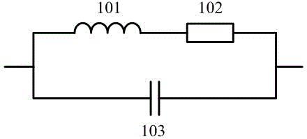
Laminated inductor

A technology of laminated inductor and laminated body, applied in the direction of inductors, fixed inductors, fixed signal inductors, etc., can solve the problems of side 202 leakage electrodes, increase of parasitic capacitance C, and inability to achieve high Q value of inductors.

Active Publication Date: 2013-01-16
SUNLORD (SHANGHAI) ELECTRONICS CO
View PDF3 Cites 1 Cited by
  • Summary
  • Abstract
  • Description
  • Claims
  • Application Information

AI Technical Summary

Problems solved by technology

However, for figure 2 As shown in the laminated inductance, the larger thickness and width of the electrode 201 will lead to the increase of the parasitic capacitance C (Q reduction) and the problem of product cracking, and the design of the electrode 201 close to the side edge of the laminate 202 will easily lead to leakage of the side 202 electrode , cracking problem, thus limiting the range of induct...

Method used


Image

  • Laminated inductor
  • Laminated inductor
  • Laminated inductor

Examples


specific Embodiment approach 1

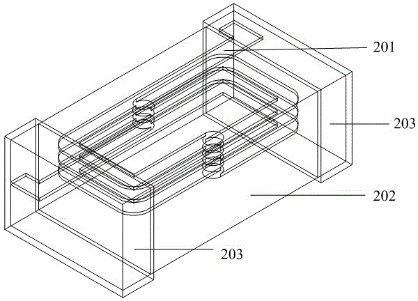
[0021] like image 3 As shown, it is a three-dimensional structure diagram of a laminated inductor according to this specific embodiment, including a laminated body 301, a coil electrode 302 and a pair of external electrodes 303, and a pair of external electrodes 303 are respectively arranged at both ends of the laminated body 301. It conducts with both lead-out ends of the coil electrode 302 .

[0022] like Figure 4 As shown, it is a schematic diagram of the exploded structure of the stacked body of the stacked inductor in this specific embodiment. The stacked body 301 includes an upper substrate 402 stacked in sequence, and multi-layer insulator layers 404, 4051-405m (in this specific embodiment m=3), 403 and the lower substrate 401 . Each insulator layer may be a ceramic body layer of ceramic material.

[0023] Wherein, the upper substrate 402 and the lower substrate 401 are also insulator layer structures, which are only used as substrates without printing conductive p...

specific Embodiment approach 2

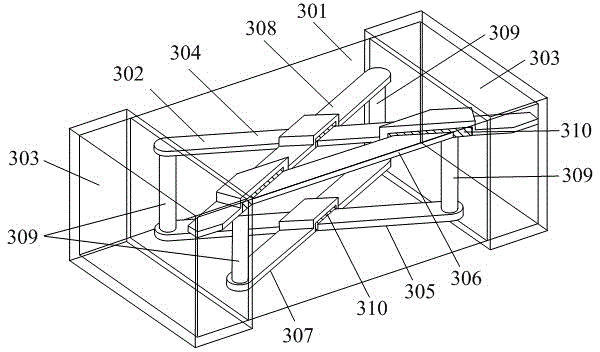
[0036] The difference between this embodiment and Embodiment 1 is that in this embodiment, n=4, that is, the uppermost insulator layer has 4 upper plane electrodes, and the lowermost insulator layer has 3 lower plane electrodes. There are 6 through-hole electrodes in the middle, and the electrodes 304 and 308 in the upper plane electrode are not arranged along the diagonal, and the electrodes 305 and 307 in the lower plane electrode are not arranged along the diagonal, and each plane electrode of the same layer is Any form of cross setting is sufficient.

[0037] like Figure 5 As shown, it is a three-dimensional structure diagram of the laminated inductor in this specific embodiment, including a laminated body 301, a coil electrode 502 and a pair of external electrodes 303, and a pair of external electrodes 303 are respectively arranged at both ends of the laminated body 301. It conducts with both lead-out ends of the coil electrode 502 .

[0038] like Image 6 As shown, i...


PUM

PropertyMeasurementUnit
Cross angleaaaaaaaaaa
Thicknessaaaaaaaaaa
Thicknessaaaaaaaaaa

Abstract

The invention discloses a laminated inductor. The laminated inductor comprises a laminating body, wherein at least the printing conducting slurry on the uppermost insulator layer in the three uppermost insulator layers of the laminating body forms n upper plane electrodes; the upper plane electrodes are alternatively arranged; insulating separating sheets are arranged at the cross positions; at least the printing conducting slurry on the lowermost insulator layer in the three lowermost insulator layers of the laminating body forms (n-1) lower plane electrodes; the lower plane electrodes are alternatively arranged; insulating separating sheets are arranged at the cross positions; 2(n-1) through holes are respectively formed in the two ends, corresponding to the lower plane electrodes, of the insulator layers except for the insulator layers with the plane electrodes; after conducting slurry laminates are coated, 2(n-1) through hole electrodes are formed; and a coil electrode is formed by connecting the upper plane electrodes, the through hole electrodes and the lower plane electrodes. The laminated inductor has relatively high Q value under each frequency, and the Q value is relatively convenient to increase and improve.

Description

technical field [0001] The invention relates to an inductance device, in particular to a laminated inductor. Background technique [0002] Multilayer inductors are often used in impedance matching or resonant circuits in radio frequency circuits (signal frequencies above 1 GHz). When selecting a multilayer inductor, in addition to the inductance parameter, the quality factor (Quality Factor, Q for short) parameter also needs to be considered. The Q value is the main parameter to measure the inductance device. It refers to the ratio of the stored energy to the consumed energy when the inductor works under an AC voltage of a certain frequency. It is expressed as the inductive reactance (the imaginary part of the impedance) and its equivalent loss. The ratio of resistances (real parts of impedance). The higher the Q value of an inductor, the smaller its losses and the higher its efficiency. [0003] like figure 1 Shown is the equivalent circuit diagram of a laminated induct...

Claims


Application Information

Patent Timeline
IPC IPC(8): H01F17/00H01F37/00H01F27/29H01F41/04
Inventor 李有云张扬王大为
Owner SUNLORD (SHANGHAI) ELECTRONICS CO
Why Eureka
Try Eureka