Semiconductor device including air gaps and method for fabricating the same

a technology of semiconductor devices and air gaps, which is applied in the direction of semiconductor devices, semiconductor/solid-state device details, electrical apparatus, etc., can solve the problems of limited parasitic capacitance reduction and deterioration of semiconductor devices performance, and achieve the effect of reducing parasitic capacitan

Active Publication Date: 2015-05-07
SK HYNIX INC
View PDF10 Cites 108 Cited by
  • Summary
  • Abstract
  • Description
  • Claims
  • Application Information

AI Technical Summary

Benefits of technology

[0007]Various embodiments are directed to a semiconductor device capable of reducing parasitic capacitance between adjacent conductive structures and a method for fabricating the same.

Problems solved by technology

An increase in parasitic capacitance may deteriorate the performance of the semiconductor device.
However, even with this method, reduction of parasitic capacitance is limited because the dielectric materials may still have too high of a high dielectric constant.

Method used


Image

  • Semiconductor device including air gaps and method for fabricating the same
  • Semiconductor device including air gaps and method for fabricating the same
  • Semiconductor device including air gaps and method for fabricating the same

Examples


first embodiment

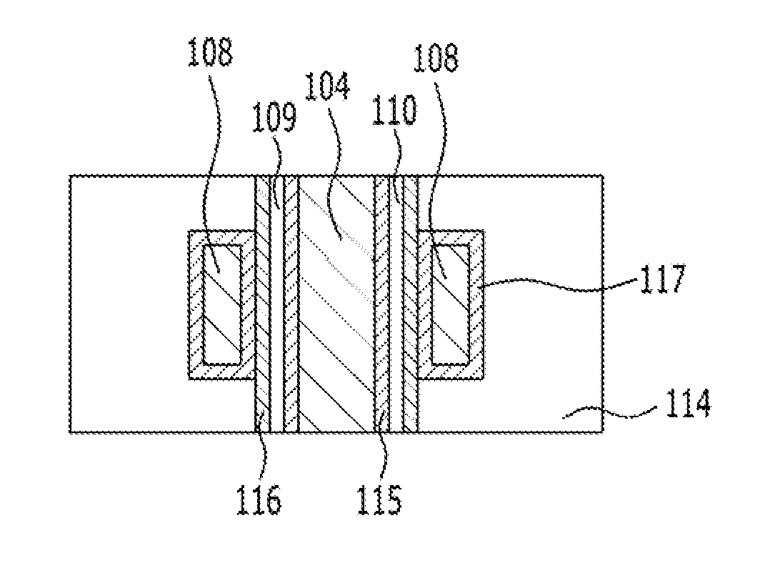
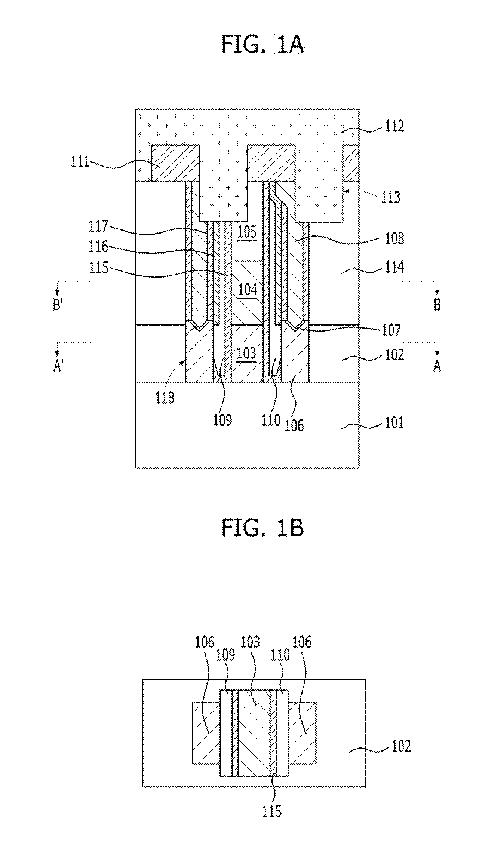
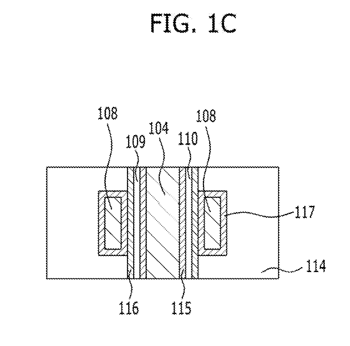
[0032]FIG. 1A is a cross-sectional view of a semiconductor device in accordance with the present invention, FIG. 1B is a plan view of line A-A′ of FIG. 1A, and FIG. 1C is a plan view of line B-B′ of FIG. 1A.

[0033]Referring to FIG. 1A, a plurality of conductive structures may be formed over a substrate 101. The conductive structures include a first conductive structure and a second conductive structure. The first conductive structure includes a first conductive pattern 103, a second conductive pattern 104, and a hard mask pattern 105. The second conductive structure includes a third conductive pattern 106, a fourth conductive pattern 107, and a fifth conductive pattern 108. A dielectric structure having air gaps 109 and 110 may be formed between the first conductive structure and the second conductive structure. The dielectric structure includes a first spacer 115, a second spacer 116, and a third spacer 117. The air gaps 109 and 110 may be formed between the first spacer 115 and the...

second embodiment

[0086]FIG. 3 is a diagram illustrating a semiconductor device in accordance with the present invention.

[0087]Referring to FIG. 3, a plurality of active regions 203 may be defined in a substrate 201 by isolation layers 202. Gate trenches 204 that cross the active regions 203 may be formed. A gate dielectric layer (not illustrated) may be formed on a surface of the gate trenches 204. Buried gate electrodes 205, which partially bury the gate trenches 204, may be formed on the gate dielectric layer. Although not illustrated, a source region and a drain region may be formed in the substrate 201. Sealing layers 206 may be formed on the buried gate electrodes 205. A bit line structure, including a bit line 208 extending in a direction crossing the buried gate electrodes 205, may be formed.

[0088]The bit line structure may include a first contact plug 207, a bit line 208, and a bit line hard mask 209. The bit line 208 may be connected to the active region 203 through the first contact plug 2...

third embodiment

[0150]FIG. 7 is a plan view illustrating a semiconductor device in accordance with the present invention. FIG. 8A is a cross-sectional view taken along line A-A′ of FIG. 7. FIG. 8B is a cross-sectional view taken along line B-B′ of FIG. 7. FIG. 8C is a detailed diagram illustrating a line-type air gap. FIG. 8D is a detailed diagram illustrating a plug-type air gap.

[0151]The semiconductor device 300 includes a plurality of buried word lines 307, a plurality of bit lines 316, and memory elements 326. The buried word lines 307 are formed within a substrate 301. The bit lines 316 are formed over the substrate 301. The buried word lines 307 and the bit lines 316 are arranged to cross each other. First plugs 315 are formed between the bit lines 316 and the substrate 301.

[0152]A stack structure of a second plug 323, an ohmic contact layer 324, and a third plug 325 is formed between each of the memory elements 326 and the substrate 301. The second plug 323 is formed between adjacent bit lin...


PUM


Abstract

Disclosed are a semiconductor device capable of reducing parasitic capacitance between adjacent conductive structures and a method for fabricating the same. The semiconductor device includes a plurality of bit line structures each comprising a first contact plug formed over a substrate and a bit line formed over the first contact plug. A spacer structure having air gaps is formed on sidewalls of the first contact plug and on sidewalls of the bit line. An plug isolation layer is formed between the plurality of bit line structures. The isolation layer includes an opening. A second contact plug is formed in the opening and a memory element is formed over the second contact plug.

Description

CROSS-REFERENCE TO RELATED APPLICATION(S)[0001]The present application claims priority of Korean Patent Application No. 10-2013-0134664 and No. 10-2014-0064625, filed on Nov. 7, 2013 and May 28, 2014, respectively, which are incorporated herein by reference in their entirety.BACKGROUND[0002]1. Field[0003]Exemplary embodiments of the present invention relate to a semiconductor device, and, more particularly, to a semiconductor device including air gaps and a method of fabricating the same.[0004]2. Description of the Related Art[0005]In general, a semiconductor device includes dielectric materials formed between adjacent conductive structures. As the degree of integration of semiconductor devices is increased, the distance between conductive structures becomes closer. For this reason, parasitic capacitance is increased. An increase in parasitic capacitance may deteriorate the performance of the semiconductor device.[0006]In order to reduce parasitic capacitance, a method for lowering ...

Claims


Application Information

Patent Timeline
Patent Type & Authority Applications(United States)
IPC IPC(8): H01L27/108H01L21/311H01L21/3213H01L21/768H01L21/02
CPCH01L27/10888H01L21/76883H01L21/76877H01L21/76802H01L21/76831H01L21/0217H01L27/1085H01L21/02164H01L21/32133H01L21/31111H01L27/10885H01L27/10876H01L21/02186H01L21/32139H01L21/76897H01L21/7682H01L21/76832H10B63/30H10B63/80H10N70/231H10N70/011H10B12/34H10B12/315H10B12/0335H10B12/053H10B12/485H01L21/764H10B12/30H01L23/5223H01L23/5226H01L23/528H01L23/535
Inventor HWANG, CHANG-YOUNKWAK, NOH-JUNGYI, HONG-GUCHOI, YUN-JEKWON, SE-HANCHOI, KI-SOOKIM, SEUNG-BUMKIM, DO-HYUNGJUNG, DOO-SUNGPARK, DAE-SIK
Owner SK HYNIX INC
Why Eureka
Try Eureka