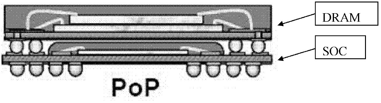
POP (Post Office Protocol) packaged SOC (System on Chip) DRAM (Dynamic Random Access Memory) input/output test method and device
A test device and chip technology, applied in static memory, instruments, etc., can solve the problems of difficult SOC chip IO testing, DRAMIO cannot be located below, and SOCIO increase.
- Summary
- Abstract
- Description
- Claims
- Application Information
AI Technical Summary
Problems solved by technology
Method used
Image

Examples
Embodiment Construction
[0033] The following description and drawings illustrate specific embodiments of the invention sufficiently to enable those skilled in the art to practice them. Other embodiments may incorporate structural, logical, electrical, process, and other changes. The examples merely represent possible variations. Individual components and functions are optional unless explicitly required, and the order of operations may vary. Portions and features of some embodiments may be included in or substituted for those of other embodiments. The scope of embodiments of the present invention includes the full scope of the claims, and all available equivalents of the claims. These embodiments of the present invention may be referred to herein, individually or collectively, by the term "invention", which is for convenience only and is not intended to automatically limit the application if in fact more than one invention is disclosed The scope is any individual invention or inventive concept.
...
PUM
 Abstract
Description
Claims
Application Information
 - R&D Engineer
- R&D Manager
- IP Professional
- Industry Leading Data Capabilities
- Powerful AI technology
- Patent DNA Extraction
Browse by: Latest US Patents, China's latest patents, Technical Efficacy Thesaurus, Application Domain, Technology Topic.
© 2024 PatSnap. All rights reserved.Legal|Privacy policy|Modern Slavery Act Transparency Statement|Sitemap