Structure and system-on-chip integration of a two-transistor and two-capacitor memory cell for trench technology

a technology of memory cell and transistor, applied in the field of structure and system-on-chip integration of two-transistor and two-capacitor memory cell for trench technology, can solve the problems of halving the cycle time, reducing the performance of commodity drams, negligible improvement of the performance of conventional embedded drams, etc., and reducing the write mode performance. , the effect of reducing the storage charge and prolonging the retention period

Inactive Publication Date: 2005-01-18
IBM CORP
View PDF4 Cites 47 Cited by
  • Summary
  • Abstract
  • Description
  • Claims
  • Application Information

AI Technical Summary

Benefits of technology

According to one aspect of the invention, there is provided a 2-port memory cell structure having two transistors and two trench capacitors coupled to a common storage node. The two transistors are independently controlled by utilizing the first and second wordlines to access a data bit in the common storage node through either one of the two transistors to the corresponding bitlines. The 2-port memory cell is structured to utilize 1-port memory cells, each having one transistor and one capacitor, while connecting the two storage nodes to a common storage node. This allows the 2-port memory cell to become fully compatible with the 1-port memory cell, thereby allo...

Problems solved by technology

y the SRAM cell. The improved performance of the conventional embedded DRAMs is negligible and is limited by the read modified write operation when it is compared to that of a similar operation in
Because the I/O width of the embedded DRAM in an embedded system can be very large, the page mode operation that is commonly used in commodity DRAMs does not improve its ...

Method used


Image

  • Structure and system-on-chip integration of a two-transistor and two-capacitor memory cell for trench technology
  • Structure and system-on-chip integration of a two-transistor and two-capacitor memory cell for trench technology
  • Structure and system-on-chip integration of a two-transistor and two-capacitor memory cell for trench technology

Examples


Embodiment Construction

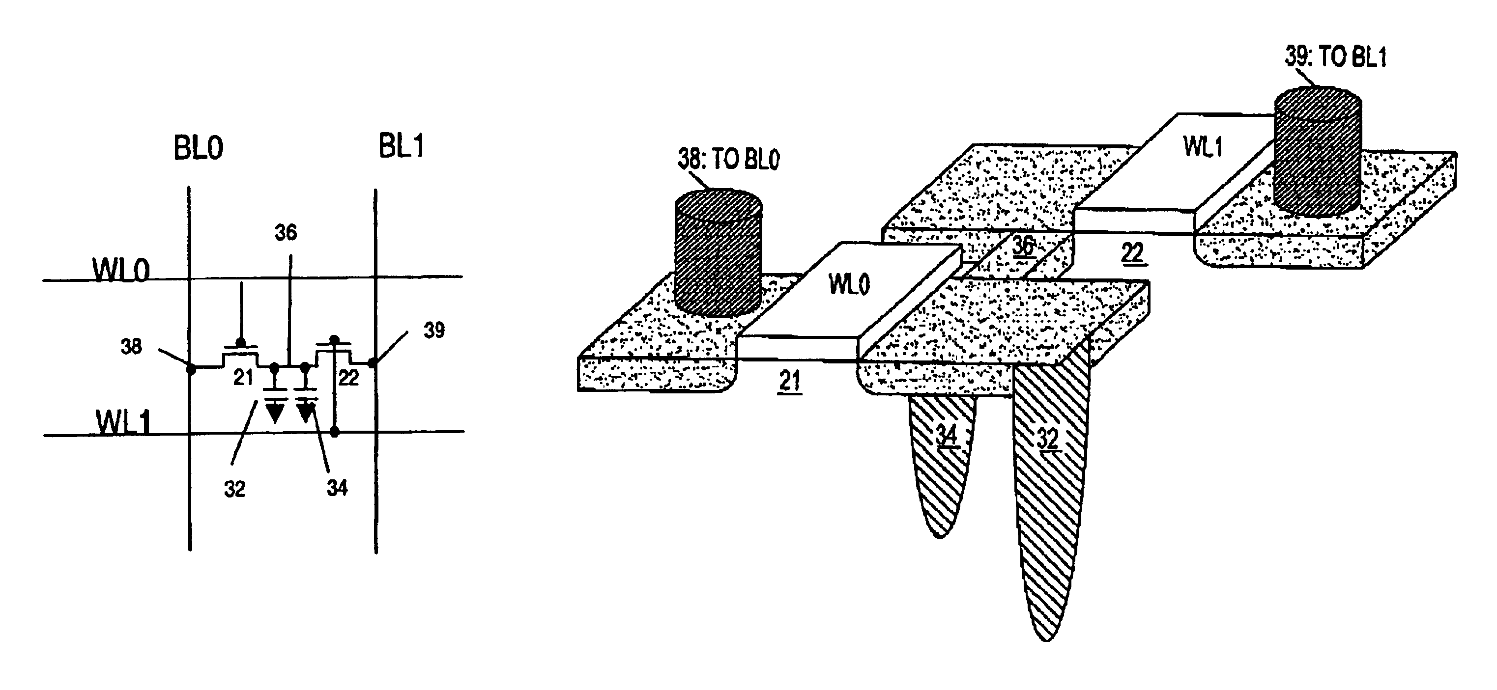
FIGS. 3A and 3B show respectively a transistor level schematic and a cross-section of the inventive 2-port memory cell when applied to trench technology.

Referring to FIG. 3A, there is shown a two-port memory cell consisting of two NMOS access transistors 21 and 22 coupled to a corresponding wordline (WL0 for port 0 and WL1 for port1) and corresponding bitline (BL0 for post 0 and BL1 for port1). Unlike a conventional 2-port memory cell having one capacitor (see FIG. 2), the 2-port memory coil includes two capacitors 32 and 34. By utilizing two transistors and two capacitors to form the cell, the structure of the inventive 2T 2C cell shown in FIG. 3A can achieve full compatibility with the 1T 1C DRAM cell shown in FIG. 1. This is achieved by coupling storage node 36 of the two 1T 1C cells by way of a diffusion connection 36, as shown in FIG. 3B, while keeping the two trench structure of the 1T 1C cell shown in FIGS. 1A and 1B. Storage node 36 can be accessed by either port 0 or post 1...


PUM


Abstract

A two-port dynamic random access memory (DRAM) cell consisting of two transistors and two trench capacitors (2T and 2C DRAM cell) connecting two one transistor and one capacitor DRAM cell (1T DRAM cell) is described. The mask data and cross-section of the 2T 2C DRAM and 1T DRAM cells are fully compatible to each other except for the diffusion connection that couples two storage nodes of the two 1T DRAM cells. This allows a one-port memory cell with 1T and 1C DRAM cell and a two-port memory cell with 2T and 2C DRAM cell to be fully integrated, forming a true system-on chip architecture. Alternatively, by halving the capacitor, the random access write cycle time is further reduced, while still maintaining the data retention time. The deep trench process time is also reduced by reducing by one-half the trench depth.

Description

BACKGROUND OF INVENTIONThis invention generally relates to embedded dynamic random access memory, and more particularly to a cell structure formed by two transistors and two capacitors to be used in a system on-chip embedded dynamic random access memory (DRAM).For several decades, one-transistor DRAMs have been the dominant choice for high density and low cost semiconductor memory in computing systems. Recently, advances in miniaturization have allowed integrating a processor on the same chip as the DRAM. Embedding a DRAM on the same chip alongside with the processor not only reduces packaging cost, but it also increases significantly the processor to memory available bandwidth. Because of the smaller memory cell size, embedded DRAMs can be approximately three to six times denser than embedded Static Random Access Memories (eSRAM) operating at lower power dissipation and 1000 times improved soft-error rate.Conventional embedded DRAM cells typically employ for commodity DRAMs a one-t...

Claims


Application Information

Patent Timeline
IPC IPC(8): G11C11/21G11C11/24H01L21/70H01L27/108H01L21/8242G11C11/401G11C11/404
CPCG11C11/404H01L27/108H01L27/10829H10B12/37H10B12/00F16L33/224F16L19/065
Inventor KIRIHATA, TOSHIAKIGOLZ, JOHN W.
Owner IBM CORP
Why Eureka
Try Eureka