Nitrided STI liner oxide for reduced corner device impact on vertical device performance

a technology of sti liner oxide and corner device, which is applied in the direction of semiconductor devices, electrical apparatus, transistors, etc., can solve the problems of depletion of channel adjacent to gate conductors, significant challenges in the manufacture of combined dram circuits, and increased thermal budg

Active Publication Date: 2006-02-14
INFINEON TECH AG +1
View PDF9 Cites 46 Cited by
  • Summary
  • Abstract
  • Description
  • Claims
  • Application Information

AI Technical Summary

Benefits of technology

[0006]It is another object of the present invention to provide an integrated method of manufacturing of vertical DRAMs with planar support devices, which reduces corner effects in the transistor portion of the DRAM.
[0011]The region adjacent the gate conductor typically contains a dopant, such as boron, and the integrated circuit device further includes an oxide layer between the gate conductor and the dopant-containing region, and extending between the isolation regions. The oxide layer and isolation regions define corner regions of the gate conductor and dopant-containing region, such that the liner reduces dopant depletion in the corner regions during subsequent thermal processing of the DRAM cell.
[0013]In another aspect, the present invention is directed to a method of fabricating an integrated circuit device comprising providing a substrate, etching a trench in the substrate and forming in the trench a dynamic random access memory (DRAM) cell. The DRAM cell has a storage capacitor at a lower end of the trench and a gate conductor overlying the storage capacitor within the trench. The method then includes doping regions in the substrate adjacent the gate conductor, and forming trenches adjacent the DRAM cell, wherein the trenches extending below the gate conductor. In the trenches there is formed an isolation liner, comprising a nitride compound, on either side of the DRAM cell, adjacent the gate conductor. The method also includes forming isolation regions in the trenches on either side of the DRAM cell. Thereafter, the DRAM cell, including the dopant-containing region adjacent the gate conductor, is subjected to elevated temperatures by thermal processing, for example, forming a support device on the substrate adjacent the isolation regions. The nitride-containing isolation liner reduces segregation of the dopant in the region adjacent to the gate conductor as a result of the thermal processing, as compared to an essentially nitrogen-free oxide-containing isolation liner. The dopant is preferably boron, and the liner preferably comprises a silicon-oxy-nitride compound.
[0015]The method may further include forming an oxide layer between the gate conductor and the dopant-containing region, and extending between the isolation regions. The oxide layer and isolation regions define corner regions of the gate conductor and dopant-containing region, and the liner reduces dopant depletion in the corner regions during subsequent thermal processing.

Problems solved by technology

However, significant challenges exist in the manufacture of combined DRAM circuits where the fabrication of embedded vertical DRAMs is integrated into the process flow of the fabrication of planar support devices.
Among these problems is the increased thermal budget, i.e., the cumulative effect of time at elevated temperature to which the implants for the vertical device are exposed.
In such case, the corner device of the transistor portion of the DRAM may be affected by the STI liner oxidation because of boron segregation into the liner, and resulting depletion in the channel adjacent the gate conductor, as a result of exposure to higher temperatures.

Method used


Image

  • Nitrided STI liner oxide for reduced corner device impact on vertical device performance
  • Nitrided STI liner oxide for reduced corner device impact on vertical device performance
  • Nitrided STI liner oxide for reduced corner device impact on vertical device performance

Examples


Embodiment Construction

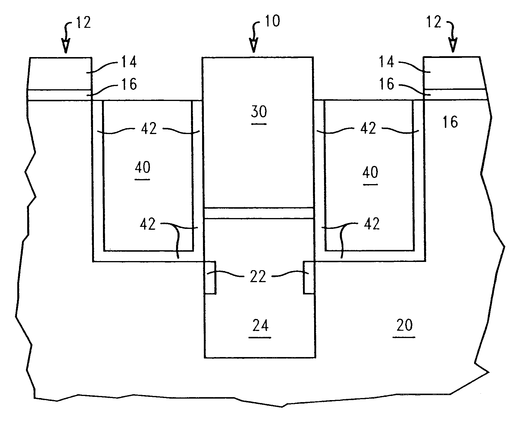
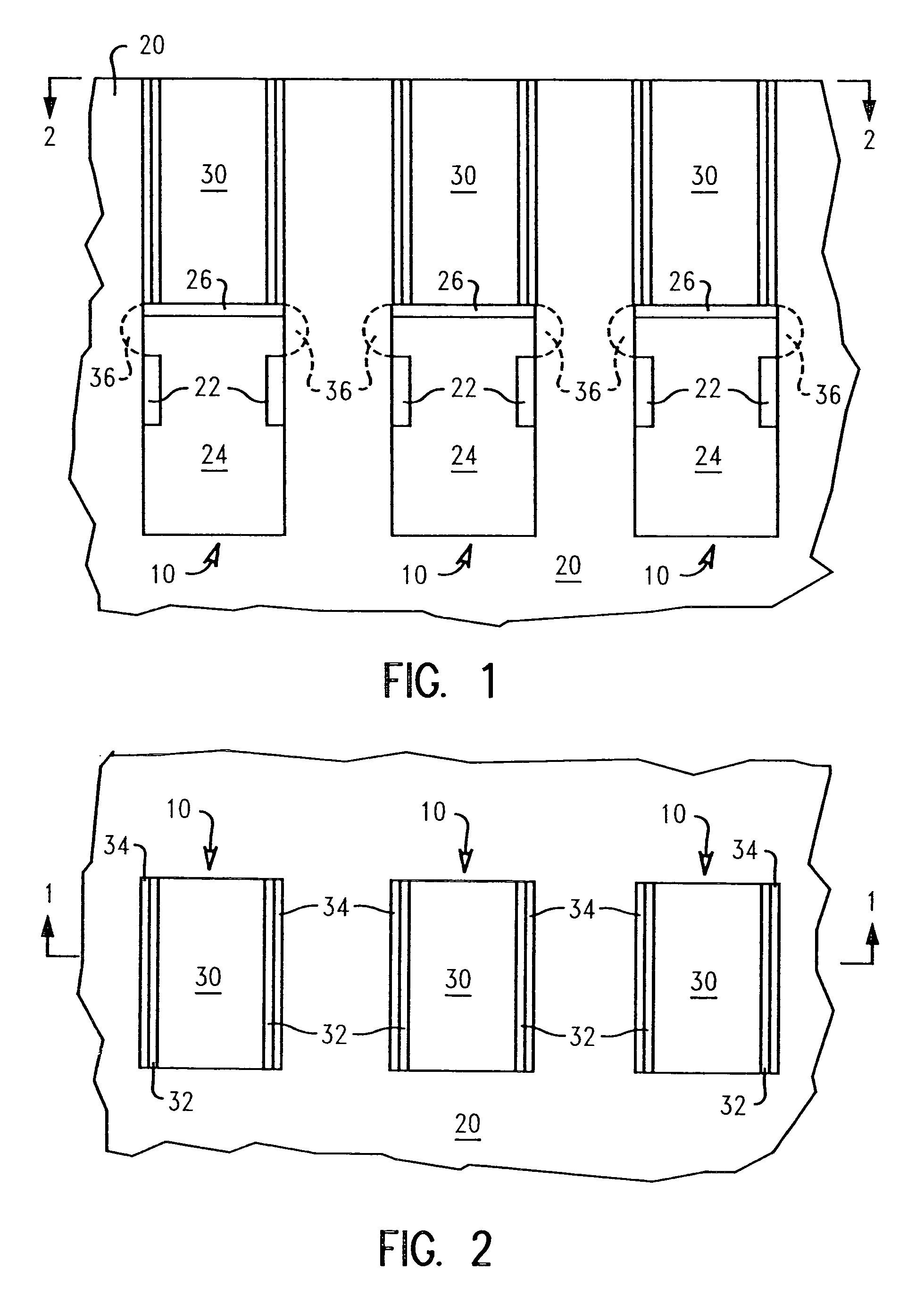
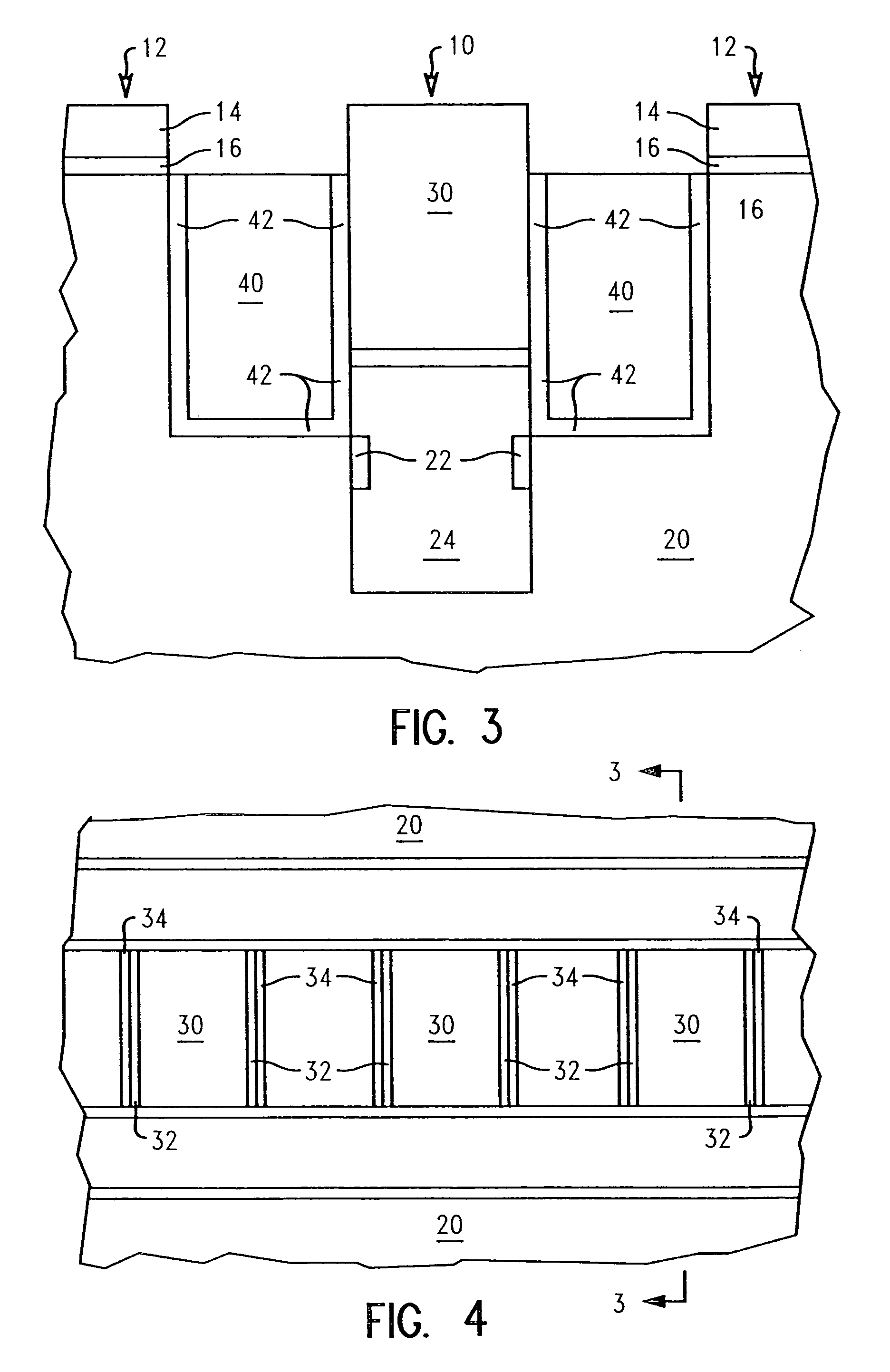
[0023]In describing the preferred embodiment of the present invention, reference will be made herein to FIGS. 1–5 of the drawings in which like numerals refer to like features of the invention. Features of the invention are not necessarily shown to scale in the drawings.

[0024]In accordance with the invention, an array of vertical DRAMs 10 are shown in elevational cross-sectional view in FIG. 1 and in plan view in FIG. 2. Each vertical DRAM 10 contains a vertical MOSFET formed in a semiconductor wafer substrate 20, preferably a silicon substrate, over a trench capacitor. In the fabrication process, a plurality of vertical deep trenches are formed from a top surface down into the silicon substrate 10 by known patterning and etching techniques. Using known processing techniques, the bottom portion of each vertical trench is then provided with a trench collar 22 of oxide surrounding a portion of doped polysilicon fill 24. The polysilicon fill 24 is completely covered with a trench top o...


PUM


Abstract

A method of fabricating an integrated circuit device comprises etching a trench in a substrate and forming a dynamic random access memory (DRAM) cell having a storage capacitor at a lower end and an overlying vertical metal oxide semiconductor field effect transistor (MOSFET) comprising a gate conductor and a boron-doped channel. The method includes forming trenches adjacent the DRAM cell and a silicon-oxy-nitride isolation liner on either side of the DRAM cell, adjacent the gate conductor. Isolation regions are then formed in the trenches on either side of the DRAM cell. Thereafter, the DRAM cell, including the boron-containing channel region adjacent the gate conductor, is subjected to elevated temperatures by thermal processing, for example, forming a support device on the substrate adjacent the isolation regions. The nitride-containing isolation liner reduces segregation of the boron in the channel region, as compared to an essentially nitrogen-free oxide-containing isolation liner.

Description

BACKGROUND OF INVENTION[0001]The present invention relates to semiconductor processing, and in particular to the fabrication of an integrated circuits having both a vertical dynamic random access memory (DRAM) and other support circuits, and including an isolation trench that reduces corner device effects in the DRAM.[0002]Vertical dynamic random access memory (DRAM) circuits have been employed to reduce effective cell size and increase memory density. Typically, a vertical DRAM memory cell comprises a vertical metal oxide semiconductor field effect transistor (MOSFET) connected to a trench capacitor below the MOSFET. In the vertical MOSFET, a surface of the channel region of the transistor is generally perpendicular to the primary surface of the substrate.[0003]DRAM circuits may be made by separating the process steps for the vertical arrays and planar support devices, e.g. logic circuits. However, significant challenges exist in the manufacture of combined DRAM circuits where the ...

Claims


Application Information

Patent Timeline
Patent Type & Authority Patents(United States)
IPC IPC(8): H01L21/8242H01L21/762H01L27/108H01L29/76
CPCH01L27/10864H01L27/10841H01L27/10894H10B12/395H10B12/0383H10B12/09
Inventor BEINTNER, JOCHENDIVAKARUNI, RAMAJAMMY, RAJARAO
Owner INFINEON TECH AG
Why Eureka
Try Eureka