Conduction structure in transparent conduction film, transparent conduction film and manufacture method thereof

A technology of transparent conductive film and conductive structure, which is applied in the direction of transparent dielectric, conductive layer on insulating carrier, printed circuit manufacturing, etc. question

Active Publication Date: 2013-01-30
ANHUI JINGZHUO OPTICAL DISPLAY TECH CO LTD
View PDF6 Cites 251 Cited by
  • Summary
  • Abstract
  • Description
  • Claims
  • Application Information

AI Technical Summary

Problems solved by technology

However, single-layer transparent conductive film is difficult to support multi-touch technology
Therefore, in order to realize the multi-touch technology, two single-layer transparent conductive films are used in the prior art, and the X and Y-axis directions are connected to each other with jumpers, which solves the shortcoming that the single-layer film does not support multi-touch, but The scheme of using two transparent conductive film structures has the following disadvantages: first, the jumper is mainly realized by yellow light, the process is complicated, and the jumper is visible on the touch screen, which will affect the appearance
Second, the development direction of the existing touch screen is light and thin. If a layer of conductive film is added, that is, a double-layer conductive film is used for touch; this will inevitably increase the thickness and the weight of itself. development trend

Method used


Image

  • Conduction structure in transparent conduction film, transparent conduction film and manufacture method thereof
  • Conduction structure in transparent conduction film, transparent conduction film and manufacture method thereof
  • Conduction structure in transparent conduction film, transparent conduction film and manufacture method thereof

Examples


Embodiment 1

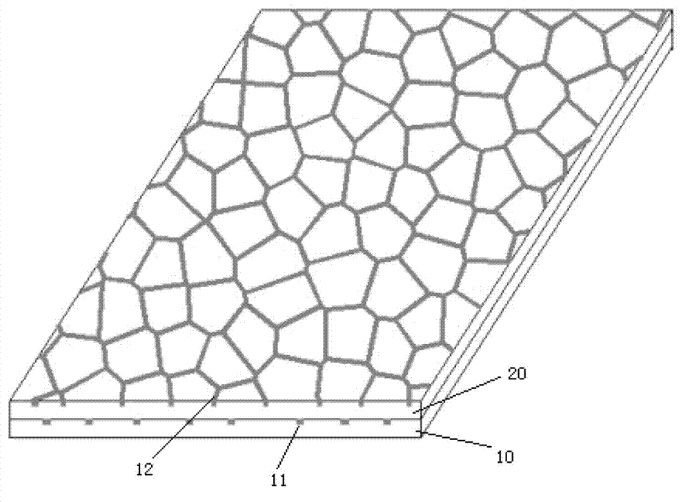
[0043] See figure 1 , figure 1It is a partial schematic diagram of the transparent conductive film according to the first embodiment of the present invention. In this embodiment, the first metal embedding layer in the conductive structure is directly formed on the substrate. As shown in the figure, the transparent conductive film includes a transparent substrate 10 and a transparent polymer layer 20 on the substrate. The conductive structure includes a grid-shaped first metal buried layer 11 disposed in the substrate 1, and a grid-shaped second metal buried layer 21 disposed in the transparent polymer layer 20, in order to ensure that the first metal buried layer 11 and the second metal buried layer 21 are insulated from each other, so that the thickness of the second metal buried layer 21 is smaller than the thickness of the polymer layer 20, so that the first metal buried layer 11 and the second metal layer 21 A part of the polymer layer 20 is separated to play an insulati...

Embodiment 2

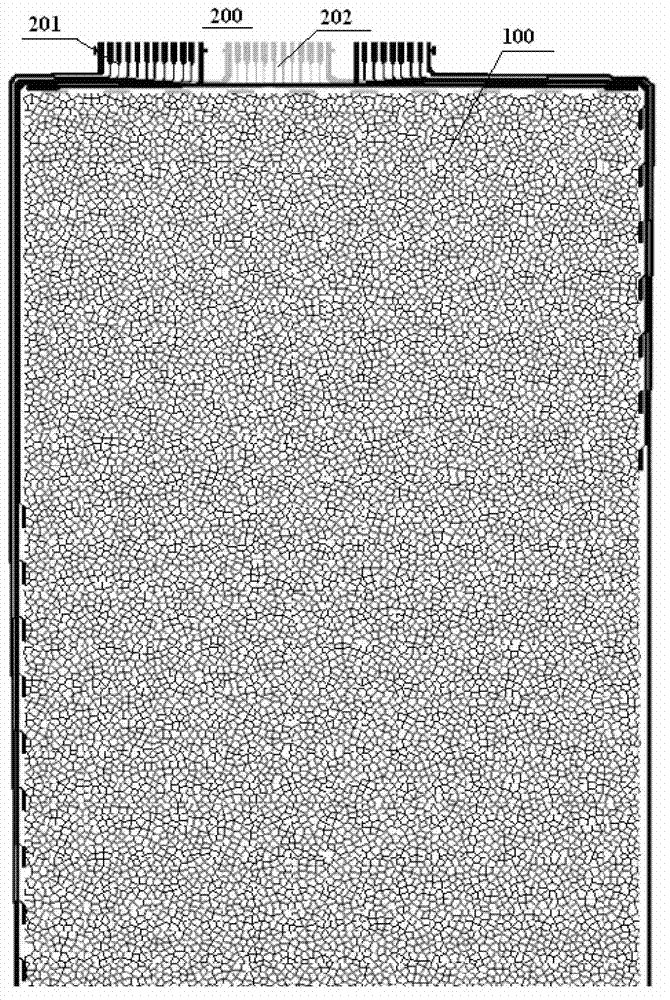
[0054] See Figure 8 , Figure 8 It is a partial schematic view of the transparent conductive film according to the second embodiment of the present invention. In this embodiment, the first metal buried layer in the conductive structure is directly fabricated in the first polymer layer on the substrate. As shown in the figure, the transparent conductive film includes a transparent substrate 10 ′, a transparent transparent film on the substrate A first polymer layer 20', and a transparent second polymer layer 30 on the first polymer layer 20'. The conductive structure includes a grid-shaped first metal buried layer 11 ′ disposed in the first polymer layer 20 ′, and a grid-shaped second metal buried layer 21 ′ disposed in the second transparent polymer layer 30 , in order to ensure the insulation between the first buried metal layer 11 ′ and the second buried metal layer 21 ′, the thickness of the second buried metal layer 21 ′ is smaller than the thickness of the second polym...


PUM

PropertyMeasurementUnit
thicknessaaaaaaaaaa

Abstract

The invention discloses a transparent conduction film, a conduction structure thereof and a preparation method of the transparent conduction film. The transparent conduction film is of a single-sided dual-layer conduction structure. The conduction structure comprises a first metal embedding layer and a second metal embedding layer, wherein the first metal embedding layer is formed by impressing on a substrate or impressing on a polymer layer on the surface of the substrate; and the second metal embedding layer is formed by coating the polymer layer on the surface of the first metal embedding layer through impressing, the first layer of conduction structure and the second layer of conduction structure have a grid groove structure, and conductive materials are filled in grooves. The single-sided graphical transparent conduction film provided by the invention has the advantages of high resolution and transmittance, independent and adjustable sheet resistance, and the like. According to the transparent conduction film, the cost can be reduced, and the weight and the thickness of a manufactured touch panel can be reduced.

Description

technical field [0001] The invention belongs to the field of multi-touch display, in particular to a transparent light guide film supporting multi-touch technology and a manufacturing method thereof. Background technique [0002] Transparent conductive film is a film with good conductivity and high light transmittance in the visible light band. At present, transparent conductive films have been widely used in fields such as flat panel displays, photovoltaic devices, touch panels, and electromagnetic shielding, and have an extremely broad market space. [0003] The ITO layer is a crucial component in the touch screen module. Although the manufacturing technology of the touch screen is developing rapidly. But taking the projected capacitive screen as an example, the basic manufacturing process of the ITO layer has not changed much in recent years. It is always inevitable to need ITO coating, ITO patterning, transparent electrode silver lead production. This traditional man...

Claims


Application Information

Patent Timeline
Patent Type & Authority Applications(China)
IPC IPC(8): H01B5/00H01B5/14H01B13/00G06F3/041
CPCG06F3/0445H05K3/1258H05K2201/0108H05K2201/09681G06F3/041G06F2203/04103H01B5/14H05K1/0213
Inventor 高育龙崔铮孙超
Owner ANHUI JINGZHUO OPTICAL DISPLAY TECH CO LTD
Why Eureka
Try Eureka