Array substrate, manufacturing and maintenance method thereof, and display device
A technology of an array substrate and a manufacturing method, which is applied in the field of display manufacturing, can solve problems such as bright spot pixel defects in pixel areas, and achieves the effects of high reliability, contributing to operation standardization, and convenience and time-saving operation standardization.
- Summary
- Abstract
- Description
- Claims
- Application Information
AI Technical Summary
Problems solved by technology
Method used
Image


Examples
Embodiment 1
[0061] This embodiment provides an array substrate, including a lead and a pixel electrode, an insulating layer is provided between the lead and the pixel electrode, the pixel electrode is separated from the lead, and the pixel electrode and the lead are conductive.
[0062] Wherein, if the display panel composed of the array substrate and the color filter substrate (that is, the display panel applied to the array substrate) is in a normally black mode (for example, the array substrate adopts the ADS mode), then the lead wire is a common electrode line or a common electrode . This is because when the normally black mode is used, when the voltage difference between the pixel electrode and the common electrode of the array substrate is zero or close to zero, the pixel area corresponding to the pixel electrode is opaque; between the pixel electrode and the common electrode When the voltage difference is large, the pixel region corresponding to the pixel electrode transmits light....
Embodiment 2
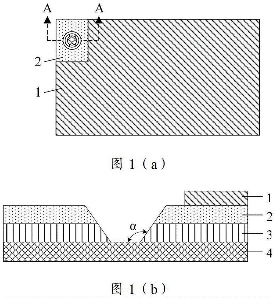
[0082] This embodiment provides an ADS mode array substrate, such as figure 1 ( figure 1 (a) and figure 1 As shown in (b), the array substrate includes a common electrode line 4, a gate insulating layer 3 disposed on the common electrode line 4, a passivation layer 2 disposed on the gate insulating layer 3, and a passivation layer disposed on the passivation layer. 2 on the pixel electrode 1. Wherein, the gate insulating layer 3 and the passivation layer 2 are provided with through holes, the relative positions of the through holes on the gate insulating layer 3 and the passivation layer 2 are the same, and the pixel electrode 1 is arranged on the passivation layer. There is no through hole on the layer 2, so that the pixel electrode 1 and the common electrode line 4 can conduct through the conductive material provided in the through hole.
[0083] exist figure 1 , the pixel electrode 1 is separated by a certain distance between the edge of the side near the through hole a...
Embodiment 3
[0096] This embodiment provides a TN mode array substrate and a maintenance method for the TN mode array substrate. The array substrate and its maintenance method are different from the array substrate and its maintenance method in Embodiment 2 in that: References to common electrode lines / common electrodes are all replaced by grid lines.
[0097] Other structures, methods and functions in this embodiment are the same as those in Embodiment 2, and will not be repeated here.
PUM
| Property | Measurement | Unit |
|---|---|---|
| angle | aaaaa | aaaaa |
Abstract
Description
Claims
Application Information