Delayed power supply circuit, power supply delay method and boosting system

A delay power supply and circuit technology, applied in the electronic field, can solve problems such as failure to achieve the purpose of boosting voltage, low input voltage, etc., and achieve the effect of ensuring the boosting effect

Active Publication Date: 2015-12-09
BOE TECH GRP CO LTD +1
View PDF2 Cites 0 Cited by
  • Summary
  • Abstract
  • Description
  • Claims
  • Application Information

AI Technical Summary

Problems solved by technology

In the traditional boost circuit, if the boost chip starts to work during the boost ramp period, it will cause the switch MOS tube in the peripheral circuit connected to the 6th pin (drive pin) of the boost chip to be turned on to the ground. , so that the input voltage will be pulled down, failing to achieve the purpose of boosting

Method used


Image

  • Delayed power supply circuit, power supply delay method and boosting system
  • Delayed power supply circuit, power supply delay method and boosting system
  • Delayed power supply circuit, power supply delay method and boosting system

Examples


Embodiment Construction

[0032] The following will clearly and completely describe the technical solutions in the embodiments of the present invention with reference to the accompanying drawings in the embodiments of the present invention. Obviously, the described embodiments are only some, not all, embodiments of the present invention. Based on the embodiments of the present invention, all other embodiments obtained by persons of ordinary skill in the art without making creative efforts belong to the protection scope of the present invention.

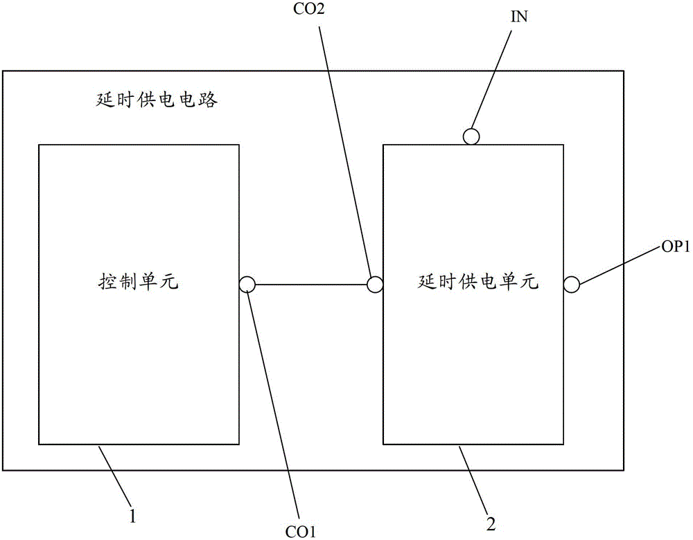
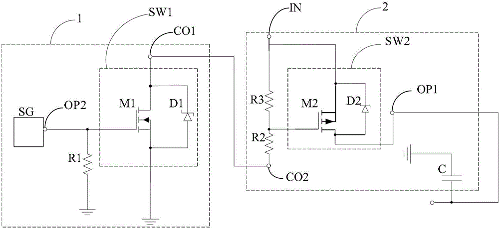
[0033] Embodiments of the present invention provide a delayed power supply circuit, such as figure 1 shown, including:

[0034] The control unit 1 includes a first control port CO1, which is connected to the delayed power supply unit 2 through the first control port CO1, and is used to control the delayed power supply unit to be turned on or off.

[0035] The delay power supply unit 2 includes a second control port CO2, an output port OP1 and a power input po...


PUM


Abstract

The embodiment of the invention provides a time-delay power supply circuit, a power supply time delay method and a boost system and relates to the field of electronics. By the embodiment of the invention, a boost chip without an enabling pin can be in a working state after a boost period of input power voltage is finished, and a boost effect of the boost chip is ensured. The time-delay power supply circuit comprises a control unit and a time-delay power supply unit, wherein the control unit comprises a first control port, and is connected with the time-delay power supply unit through the first control port and used for controlling the switch-on and switch-off of the time-delay power supply unit; the time-delay power supply unit comprises a second control port, an output port and a power input port; the second control port is connected with the first control port; the power input port is connected with a power supply; and the output port is connected with the input end of the boost chip and used for outputting the stabilized voltage of the power supply to the boost chip after the boost period of the power voltage is finished and a switch-on signal of the control unit is received. The embodiment of the invention is applicable to power supply of the boost chip.

Description

technical field [0001] The invention relates to the field of electronics, in particular to a delay power supply circuit, a power supply delay method and a voltage boosting system. Background technique [0002] A general boost chip has two pins, Vin power input and EN enable. In actual use, some classic boost chips only have a Vin pin, without a separate EN pin. From a functional point of view, after the Vin pin reaches the recognition level of the chip, the boost chip starts to work, that is, the two pins are combined into one. [0003] In actual use, the input voltage of the Vin pin of the boost chip does not reach the required voltage immediately, but needs a certain ramp-up time, and the input voltage of the boost chip does not actually reach the required voltage during this period of time. required voltage. In the traditional boost circuit, if the boost chip starts to work during the boost ramp period, it will cause the switch MOS tube in the peripheral circuit connec...

Claims


Application Information

Patent Timeline
Patent Type & Authority Patents(China)
IPC IPC(8): H02M1/36
Inventor 王立岩
Owner BOE TECH GRP CO LTD
Why Eureka
Try Eureka