Analog-to-digital conversion device and analog-to-digital conversion method

A technology of analog-to-digital conversion and data sampling, which is applied in the direction of analog-to-digital converters, etc., can solve the problems of signal distortion, lengthening of sampling time, and keeping voltage drop, etc., to achieve the effect of ensuring work reliability, simple device structure, and ensuring reliability

Active Publication Date: 2013-02-13
PEKING UNIV
View PDF2 Cites 11 Cited by
  • Summary
  • Abstract
  • Description
  • Claims
  • Application Information

AI Technical Summary

Problems solved by technology

The traditional sample-and-hold circuit includes a sampling switch and a holding capacitor, but storing the sampling signal through the holding capacitor has the disadvantage of holding a voltage drop
Because the capacitor always has a discharge path, the output voltage drops during the hold period, resulting in signal distortion. Although increasing the capacitor capacity can reduce the voltage drop, it will increase the sampling time.
In addition, in integrated circuit design, the design and implementation of capacitors face some inherent difficulties: for ordinary small capacitors, the source and drain of MOS transistors are connected to realize, and the volume of such a capacitor is the volume of a switch
Although there are many designs to reduce the volume of capacitors, these methods usually consume a considerable amount of volume in integrated circuits.

Method used


Image

  • Analog-to-digital conversion device and analog-to-digital conversion method
  • Analog-to-digital conversion device and analog-to-digital conversion method
  • Analog-to-digital conversion device and analog-to-digital conversion method

Examples


Embodiment Construction

[0033] The specific implementation manners of the present invention will be further described in detail below in conjunction with the accompanying drawings and embodiments. The following examples are used to illustrate the present invention, but are not intended to limit the scope of the present invention.

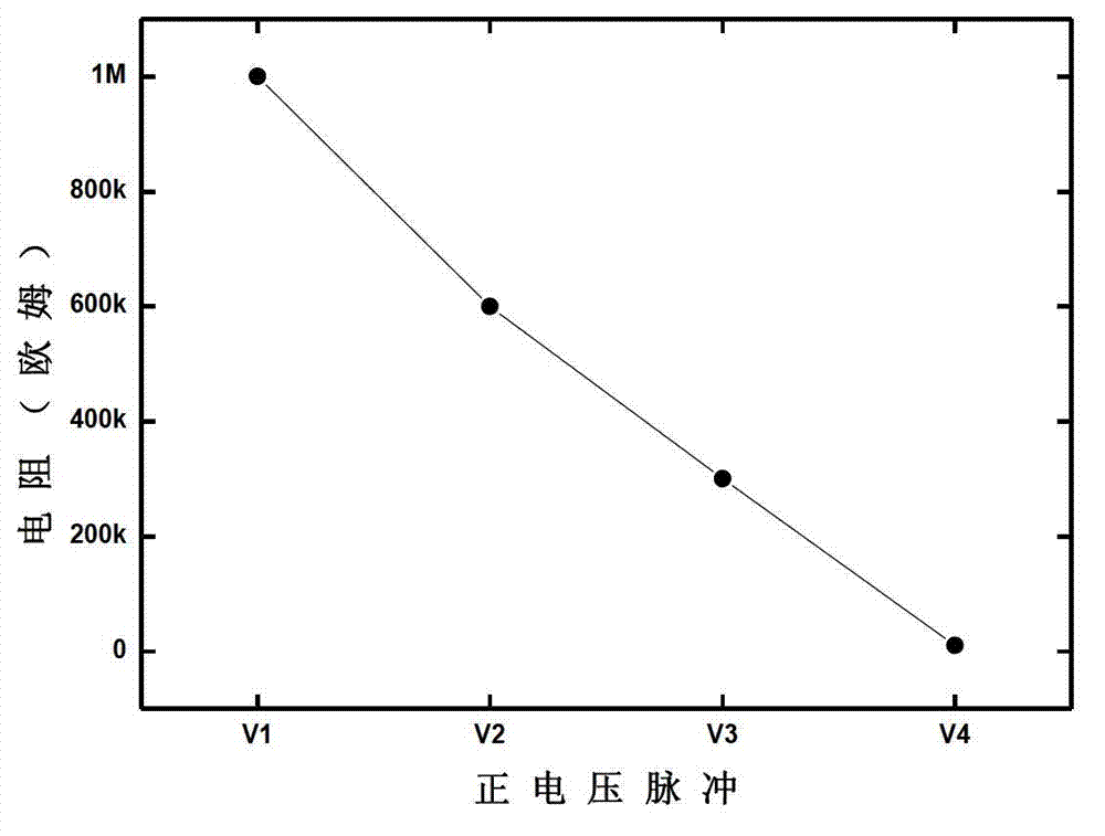
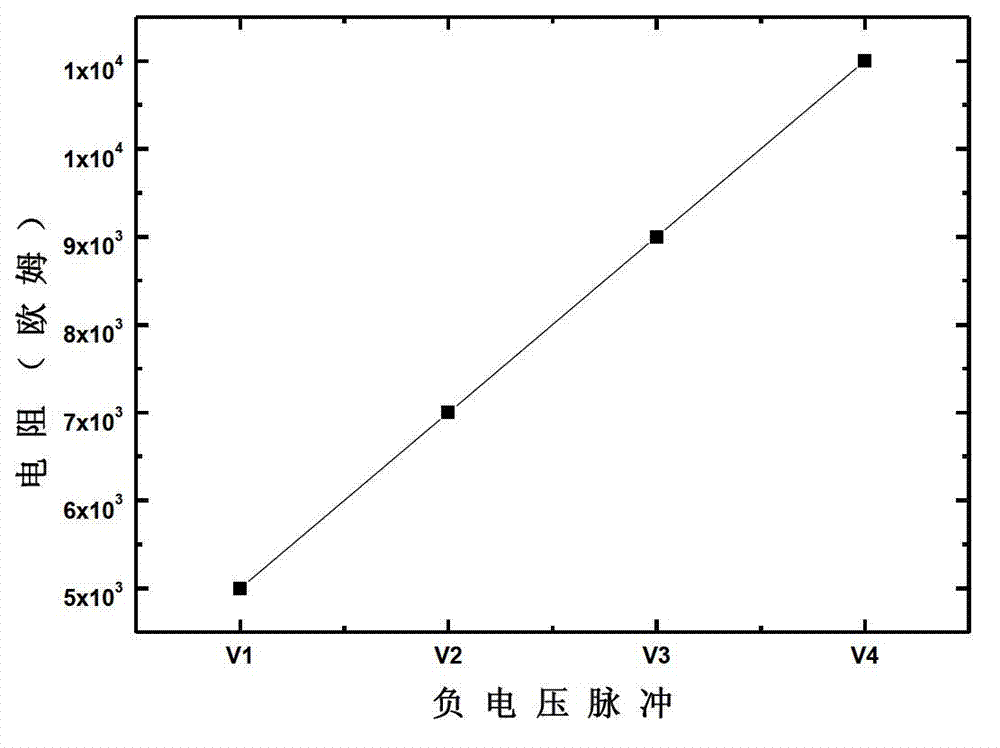
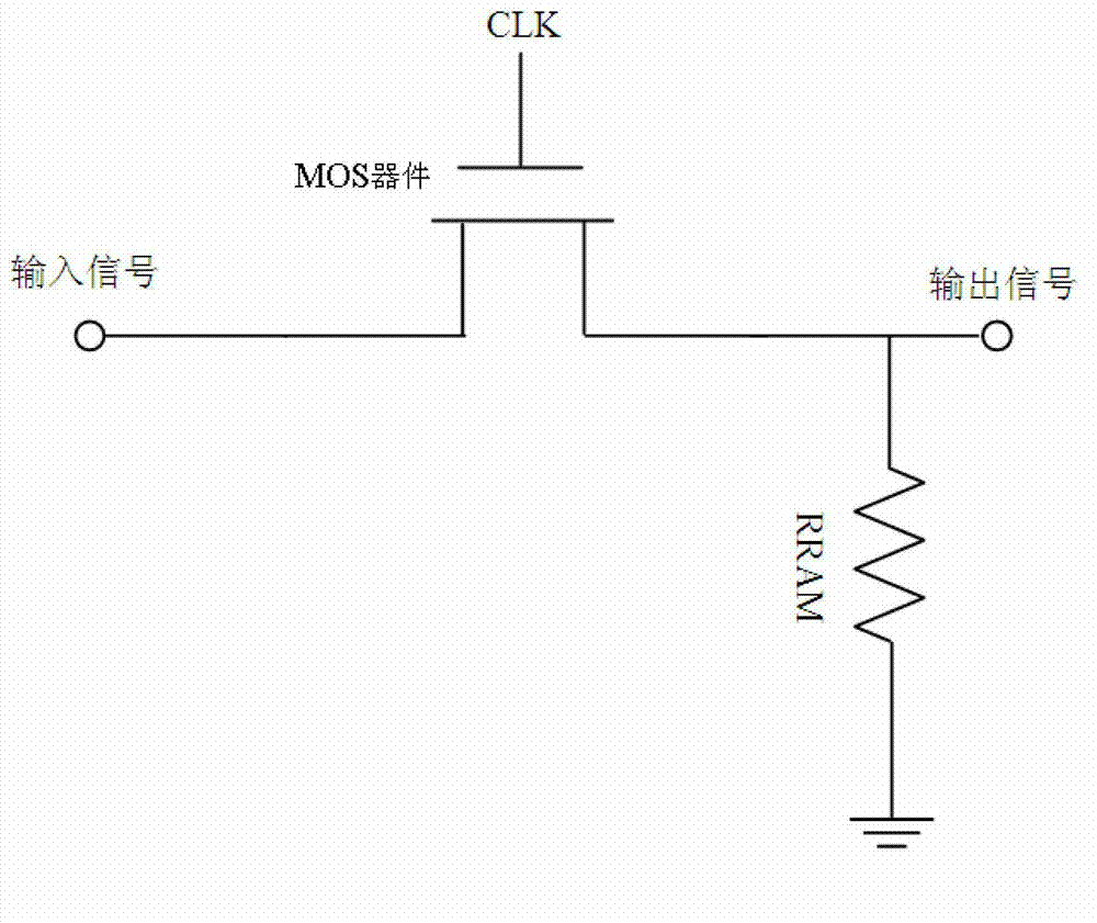
[0034] Using resistance changes, a new type of non-volatile memory called "Resistive RAM (RRAM)" has the advantages of high speed (<1ns), low operating voltage (<1V), high storage density, and CMOS process compatibility. A strong contender for next-generation semiconductor memory. The working mode of the resistive variable memory includes two kinds of unipolar and bipolar. The former applies a single-polarity voltage at both ends of the device, and uses the difference in the applied voltage to control the resistance value of the resistive variable material to switch between high and low resistance states to realize data storage. Writing and erasing; the latter uses voltag...


PUM


Abstract

The invention relates to the technical field of a semiconductor integrated circuit and manufacturing thereof and discloses an analog-to-digital conversion device and an analog-to-digital conversion method. The analog-to-digital conversion device comprises a data sampling and holding unit, a quantizing unit and an encoding unit, wherein the data sampling and holding unit is used for carrying out data sampling to obtain an analog voltage signal and storing the analog voltage signal; the quantizing unit is used for quantizing the analog voltage signal output by the data sampling and holding unit; the encoding unit is used for encoding data output by the quantizing unit to obtain a digital signal; and the data sampling and holding unit comprises a resistance random access memory. According to the invention, the data storage (or holding) in the analog-to-digital conversion process is implemented by utilizing the resistance random access memory; and experiments show that data holding time can reach 10 years, and thus, the data reliability can be ensured, so that the operational reliability of the analog-to-digital conversion device is also ensured. Moreover, the device disclosed by the invention has a simple structure and is low in cost.

Description

technical field [0001] The invention relates to the technical field of semiconductor integrated circuits and their manufacture, in particular to an analog-to-digital conversion device and an analog-to-digital conversion method. Background technique [0002] The circuit that converts analog signals into digital signals is called an analog-to-digital converter (Analog to Digital Converter), that is, an A / D converter. The mutual conversion between analog signal and digital signal is of great significance. First of all, digital signals have the advantages of simple structure, strong anti-interference ability, good stability, high degree of automation in design and testing, and easy realization of large-scale integration. Using digital signals to process analog signals in signal transmission, processing, storage, output and display Confidentiality and other aspects have very obvious advantages. Secondly, with the advancement of integrated circuit technology and the rapid develo...

Claims


Application Information

Patent Timeline
Patent Type & Authority Applications(China)
IPC IPC(8): H03M1/12
Inventor 康晋锋刘睿陈冰张飞飞刘力锋刘晓彦
Owner PEKING UNIV
Why Eureka
Try Eureka