Pad Pattern Repair Equipment

A welding pad and equipment technology, applied in the field of welding pad pattern repair equipment, can solve problems such as reducing the process qualification rate, and achieve the effect of improving the process qualification rate

Active Publication Date: 2016-09-28
苏州科韵激光科技有限公司
View PDF4 Cites 0 Cited by
  • Summary
  • Abstract
  • Description
  • Claims
  • Application Information

AI Technical Summary

Problems solved by technology

[0004] In particular, because of scratches in the contact area of ​​the probe tip when performing probe station testing or because of scratches caused by particles generated during glass scribing or glass cutting steps or during loading / unloading of other substrates Defects occur in the pad 16 due to scratches and particles
[0005] However, since the gap between the substrate and the chamber, which is traditionally used for repairing, remains unchanged, the air in the repaired area will flow out of the outside due to the pressure difference between the repaired area and the outside, reducing the process yield

Method used


Image

  • Pad Pattern Repair Equipment
  • Pad Pattern Repair Equipment
  • Pad Pattern Repair Equipment

Examples


Embodiment Construction

[0038] An embodiment of the pad pattern repairing device according to the present invention will be described below with reference to the accompanying drawings.

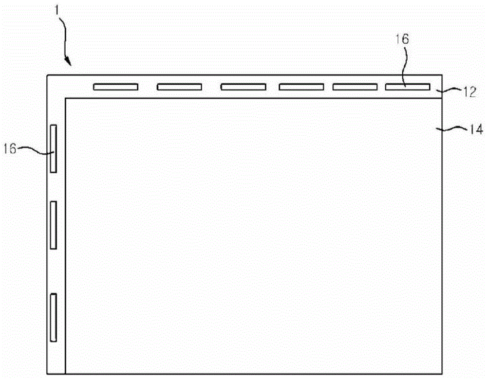
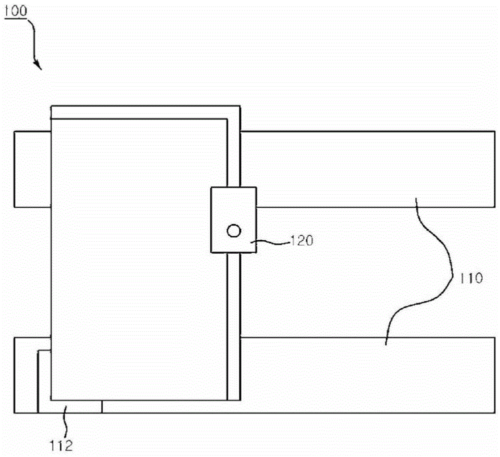
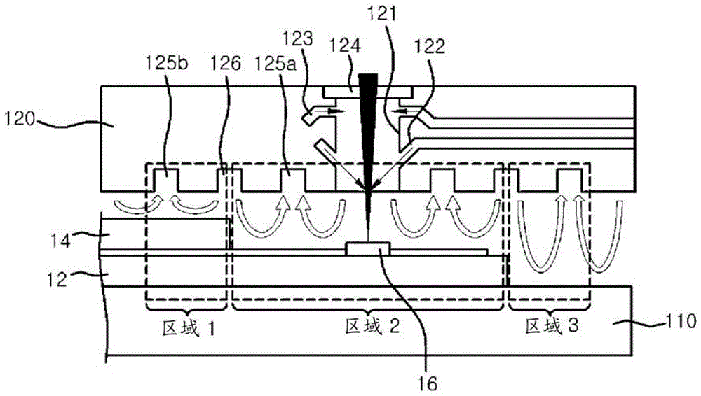
[0039] Such as figure 2 and image 3 As shown, a pad pattern repairing device 100 according to a preferred embodiment of the present invention includes a step 110, a chamber 120, and a driving part and a clamp 130, providing a signal that will be applied to a TFT substrate 12 and a color filter substrate 14 has the function of repairing defects in the electrodes of the bonding pads 16 of the non-overlapping TFT substrate 12 .

[0040] In particular, the pad pattern repairing apparatus 100 relates to a pad 16 that connects an LCD or OLED substrate (hereinafter referred to as "substrate") with a driving printed circuit board (PCB) and relates to an application for repairing a metal electrode that occurs in the pad 16. Open or short defect laser chemical vapor deposition (CVD) repair equipment.

[0041] The substrat...


PUM


Abstract

The present invention relates to a pad pattern repair apparatus. The present invention provides an apparatus for repairing defects in pad electrodes equipped for applying signals to one of multiple substrates, comprising a stage into the reference surface of which the substrate is loaded; a chamber where a first exhaust, a shield gas outlet, and a second exhaust are formed sequentially in the lower surface of the chamber with respect to a laser light emission hole being equipped on the stage and moving to the defect position of the pad electrode and having structure to discharge purifying gas and raw gas in the middle of the hole; and a clamp being installed on the stage and supporting the opposite surface of a substrate adhered closely to the reference surface, the gap between the substrate and the lower surface of the chamber varying in the inside and outside of the lower surface of the chamber. A pad pattern repair apparatus according to the present invention maintains the pressure in the area where repairing a defect is carried out at a constant level, improving a process yield.

Description

technical field [0001] The present invention relates to a pad pattern repairing device, and more particularly to a pad pattern repairing device for repairing a defect in a pad electrode, the pad pattern repairing device being installed at a color filter substrate and used for inputting a detection signal. Background technique [0002] figure 1 The structure of a conventional LCD panel 10 is shown, which includes detection signal input pads 16 contacted with probe pins of a probe unit for visual inspection and OLB pads contacted with detection signal input pads at the time of overall testing. 16. The detection signal input pad is composed of a TFT substrate 12 and a color filter substrate 14 combined in a laminated form. [0003] The bonding pad 16 maintains a structure in which a TAG film, an anisotropic conductive film (ACF), an LDI (LCD driver IC), and glass are laminated together one above the other. [0004] In particular, because of scratches in the contact area of ​​...

Claims


Application Information

Patent Timeline
Patent Type & Authority Patents(China)
IPC IPC(8): G01R1/06H01L21/66G02F1/1345
CPCG02F1/1309G02F1/13458G02F1/136259H01L22/32
Inventor 金仙株金宇珍朴成勋李孝成
Owner 苏州科韵激光科技有限公司
Why Eureka
Try Eureka