Package structure and manufacturing method thereof

A technology of packaging structure and manufacturing method, which is applied in semiconductor/solid-state device manufacturing, semiconductor/solid-state device components, semiconductor devices, etc., can solve problems such as insufficient strength and warpage of the overall structure, and achieve improved reliability and improved reliability. Process pass rate, warpage prevention effect

Active Publication Date: 2020-08-18
UNIMICRON TECH CORP
View PDF4 Cites 0 Cited by
  • Summary
  • Abstract
  • Description
  • Claims
  • Application Information

AI Technical Summary

Problems solved by technology

However, since the load-bearing plate without core layer lacks a hard core plate for support, resulting in insufficient strength, the overall structure is prone to warpage

Method used


Image

  • Package structure and manufacturing method thereof
  • Package structure and manufacturing method thereof
  • Package structure and manufacturing method thereof

Examples


Embodiment Construction

[0021] A number of implementations of the present invention will be disclosed below with the accompanying drawings. For the sake of clarity, many practical details will be described together in the following description. It should be understood, however, that these practical details should not be used to limit the invention. That is, in some embodiments of the present invention, these practical details are unnecessary. In addition, for the sake of simplifying the drawings, some well-known and commonly used structures and elements will be shown in a simple and schematic manner in the drawings.

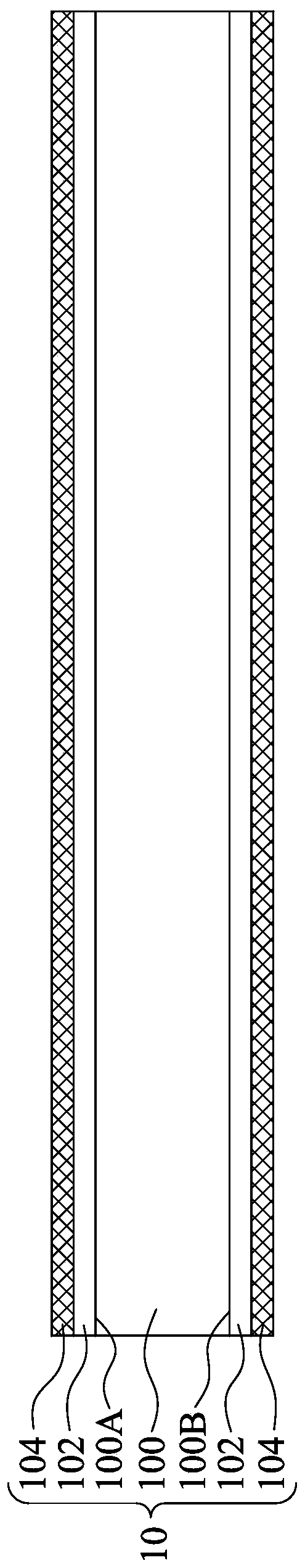
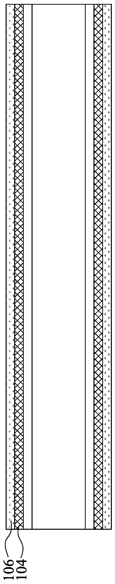
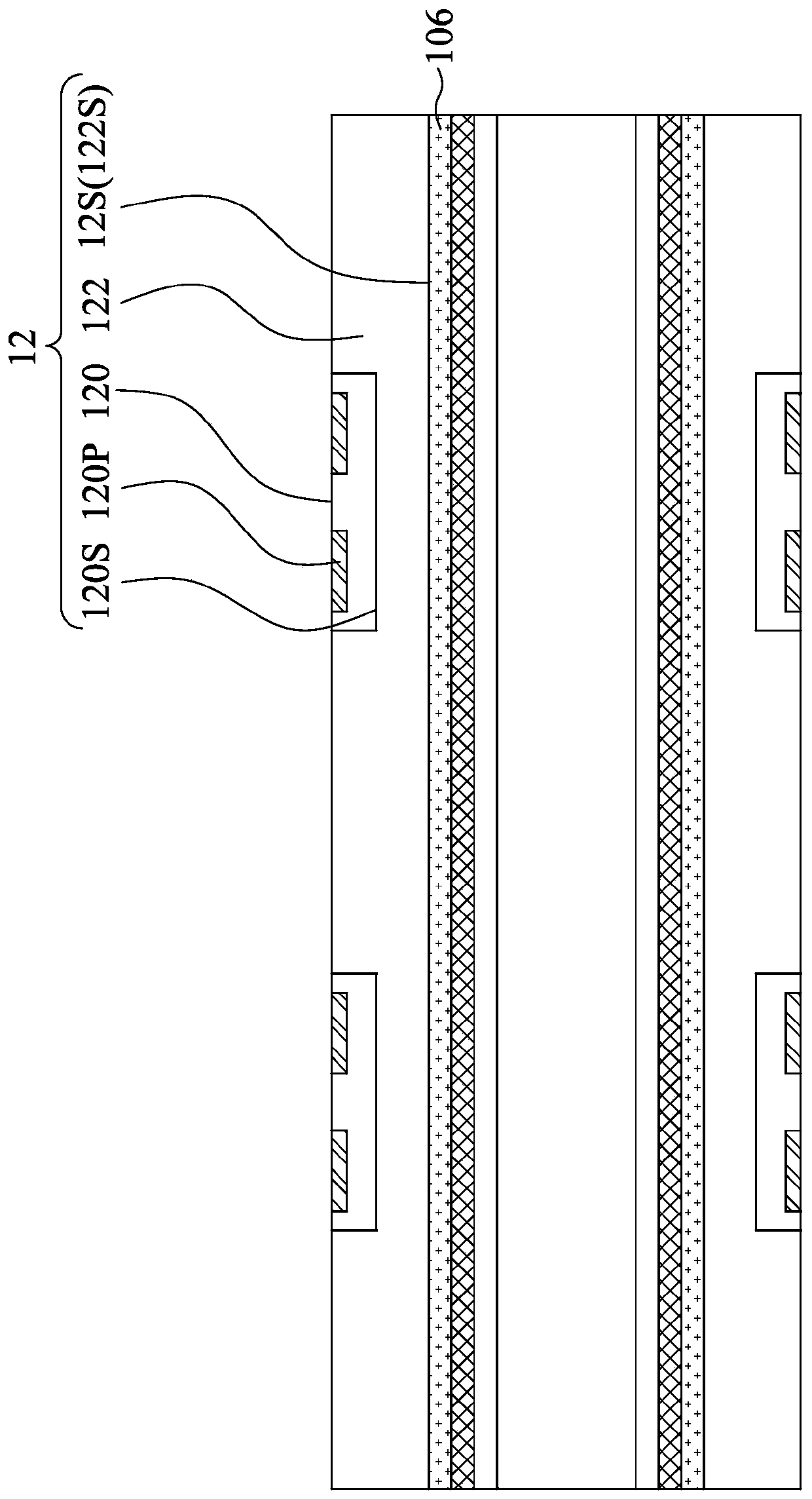
[0022] Figure 1A ~ Figure 1G It is a cross-sectional view of each step of the manufacturing method of the package structure 18 according to an embodiment of the present invention. First, if Figure 1A As shown, a carrier board 10 is provided, and the carrier board 10 includes a support layer 100 having two opposite surfaces 100A, 100B, a peeling layer 102 disposed on the opposing two...


PUM

PropertyMeasurementUnit
thicknessaaaaaaaaaa

Abstract

The invention discloses an encapsulation structure and a manufacturing method thereof. The encapsulation structure comprises a metal layer, a composite layer of a non-conductor inorganic material and an organic material, a sealant, a wafer, a circuit layer structure and an insulating protection layer. The composite layer of non-conductive inorganic material and organic material is arranged on the metal layer. The sealant is combined on the composite layer of non-conductive inorganic material and organic material. The chip is embedded in the encapsulant, and the chip has a plurality of electrode pads. The wiring layer structure is formed on the encapsulant and the wafer. The circuit layer structure includes at least one dielectric layer and at least one circuit layer, the dielectric layer has a plurality of conductive blind holes, the circuit layer is located on the dielectric layer, and the bottommost circuit layer is electrically connected to the electrode pad through the conductive blind holes. The insulation protection layer is formed on the circuit layer structure. The insulating protection layer has a plurality of openings, so that part of the surface of the circuit layer structure is exposed in the openings. The invention can strengthen the overall structural strength to prevent warpage.

Description

technical field [0001] The invention relates to a packaging structure and a manufacturing method thereof. Background technique [0002] With the evolution of semiconductor packaging technology, in addition to the traditional wire bonding (Wire bonding) semiconductor packaging technology, different packaging types have been developed for semiconductor devices, such as directly embedding in the package substrate. And electrically integrate semiconductor chips with integrated circuits to reduce the overall volume and improve electrical functions. [0003] In order to meet the requirements of shortening the length of wires, reducing the thickness of the overall structure, and responding to the trend of high frequency and miniaturization, a method of processing embedded chip substrates based on a coreless carrier board has been developed. However, since the load-bearing board without a core layer lacks a hard core board body for support, the strength is insufficient, and thus th...

Claims


Application Information

Patent Timeline
Patent Type & Authority Patents(China)
IPC IPC(8): H01L23/498H01L21/48
CPCH01L23/49811H01L23/49894H01L21/481H01L21/4853H01L2224/18H01L2224/73267H01L2224/04105H01L2224/96
Inventor 杨凯铭林晨浩蔡王翔柯正达
Owner UNIMICRON TECH CORP
Why Eureka
Try Eureka