Detection device and detection method for internal defects of silicon wafer

A detection device and internal defect technology, which is applied in the direction of optical testing for flaws/defects, etc., can solve the problems of shortened service life, waste, and loss of solar cells, and achieve comfortable and convenient operation, convenient silicon wafers, and reduced losses.

Inactive Publication Date: 2013-03-06
SHANGHAI OPTECH TECH CARVE OUT
View PDF3 Cites 15 Cited by
  • Summary
  • Abstract
  • Description
  • Claims
  • Application Information

AI Technical Summary

Problems solved by technology

[0003] Therefore, solar energy, a green energy, is favored by the majority of people; solar cells must undergo relevant testing before leaving the factory, otherwise, once defective products enter the market, problems such as shortened service life of solar cells and insufficient power generation will occur. It c

Method used


Image

  • Detection device and detection method for internal defects of silicon wafer

Examples


Embodiment Construction

[0023] The technical characteristics of the present invention will be further elaborated below in conjunction with the accompanying drawings and specific embodiments.

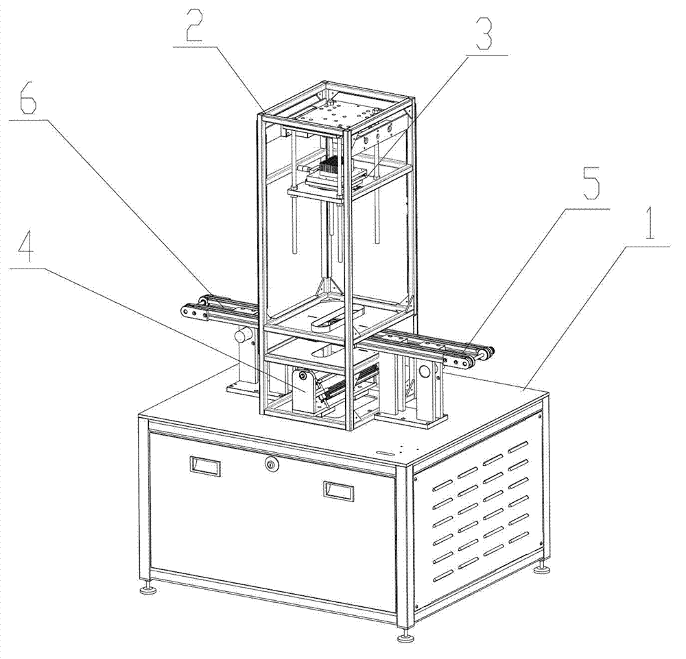
[0024] Such as figure 1 The device for detecting internal defects of a silicon wafer includes a detection module casing 1 forming a darkroom, the front of the detection module casing 1 is an operation table, and a test frame 2 is arranged on the detection module casing 1; The three-dimensional space adjustment of up and down, left and right, front and rear and rotation angle, and the detector adjustment module 3 fixed on the upper part of the test frame; it has the three-dimensional space adjustment of up and down, left and right, front and back and rotation angle of the line light source, and is fixed on the test frame. The lower linear light source adjustment module 4; and the loading conveyor platform 5 and the unloading conveyor platform 7 fixed on the detection module shell 1 through brackets; and necessar...


PUM

PropertyMeasurementUnit
Thicknessaaaaaaaaaa

Abstract

The invention discloses a detection device and a detection method for internal defects of a silicon wafer. The detection device comprises a detection module shell forming a darkroom, wherein the front of the detection module shell is provided with an operating board, and the detection module shell is provided with a test frame; the detection device further comprises a probe adjusting module, a line light source adjustment module, a loading conveying platform, an unloading conveying platform, and a necessary electrical control circuit and a power supply. The probe adjusting module can carry out three-dimensional spatial adjustment, including up-down adjustment, left-right adjustment, front-back adjustment and rotation angle adjustment, on a probe, and is fixed on the upper part of the test frame; the line light source adjustment module carries out three-dimensional spatial adjustment, including up-down adjustment, left-right adjustment, front-back adjustment and rotation angle adjustment, on the line light source, and is fixed at the lower part of the test frame; and the upper loading conveying platform and the lower unloading conveying platform are fixed on the detection module shell via a bracket. The detection device and the detection method can be used for breaking through the condition of uneven outgoing quality of the wafers in the past, and greatly reducing a series of defects of the wafers caused by the quality problem.

Description

technical field [0001] The invention relates to a silicon chip internal defect detection device and a detection method thereof, which is a visual detection method and belongs to the field of silicon chip detection. Background technique [0002] In the past few years, China's energy production has been growing rapidly. By the 21st century, China has the world's third largest energy production system, but the form of energy supply is not optimistic. In the context of heavy industry and large population, my country is even facing increasingly serious problems. The problem of energy use and supply, the solution of energy shortage is imminent. [0003] Therefore, solar energy, a green energy, is favored by the majority of people; solar cells must undergo relevant testing before leaving the factory, otherwise, once defective products enter the market, problems such as shortened service life of solar cells and insufficient power generation will occur. It causes huge waste and loss....

Claims


Application Information

Patent Timeline
IPC IPC(8): G01N21/88
Inventor 王振黄海生吴国辉
Owner SHANGHAI OPTECH TECH CARVE OUT
Why Eureka
Try Eureka