


Quick Research
Generate reliable direction feasibility study reports for your R&D in just a few steps.

Technical Q&A
Discover and master advanced knowledge NOW. Basics, ideas, possibilities, all at once.

Find Solutions
As an expert in R&D theories, this can generate solutions to your technical problems instantly.

Evaluate Feasibility
Analyze your overall solution with one click, know your potential R&D risks in advance.

Monitor Landscape
Get weekly tech updates, stay abreast of the latest tech innovations and key insights.
Electrostatic discharge protective circuit and driving method and display panel
An electrostatic discharge and driving method technology, which is applied to emergency protection circuit devices, emergency protection circuit devices, circuit devices and other directions for limiting overcurrent/overvoltage, and can solve the problems of low opening degree of TFTB403 and slow current leakage.
- Summary
- Abstract
- Description
- Claims
- Application Information
AI Technical Summary
Problems solved by technology
Method used
Image

Examples
Embodiment 1
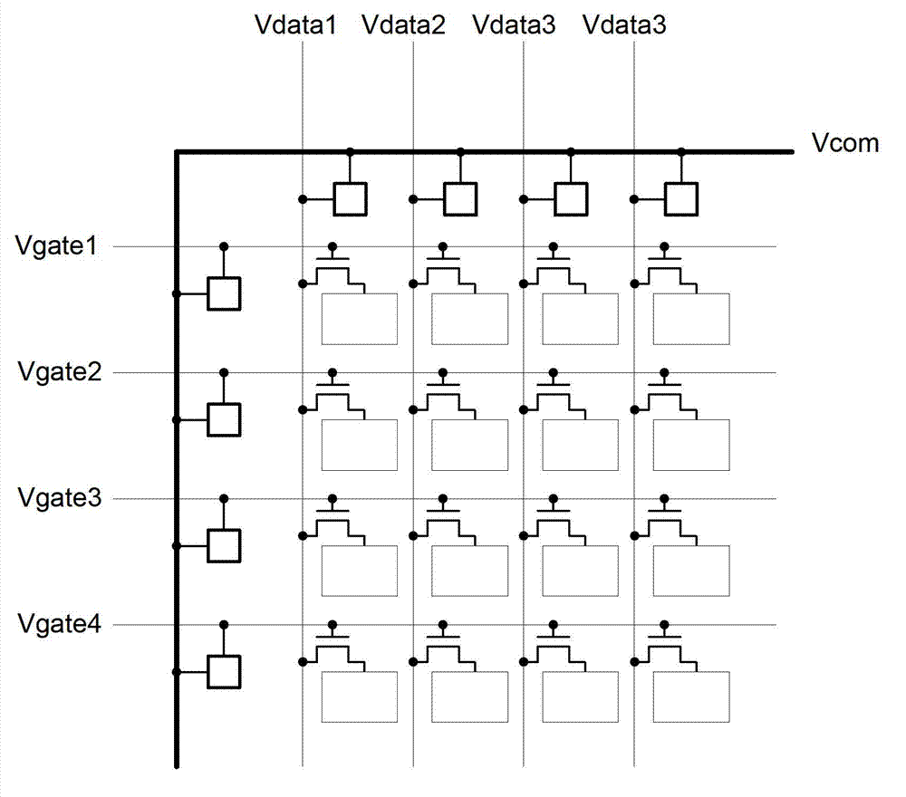
[0047] see Figure 7 , an ESD protection circuit provided by an embodiment of the present invention includes:
[0048] The first thin film transistor 101, the drain of which is connected to the data signal terminal V data , the source and gate are connected as node V net , connected to the drain of the fourth thin film transistor 104;
[0049] The second thin film transistor 102, its drain is connected to the first power voltage terminal VGH, and its source is connected to the data signal terminal V data , the gate is connected to the node V net ;
[0050] The third thin film transistor 103, its drain is connected to the data signal terminal V data , the source is connected to the second power voltage terminal VGL, and the gate is connected to the third power voltage terminal VGL2;
[0051] The source and gate of the fourth thin film transistor 104 are connected to the second power voltage terminal VGL;
[0052] Bootstrap capacitor C1 is located at node V net and data ...
Embodiment 2
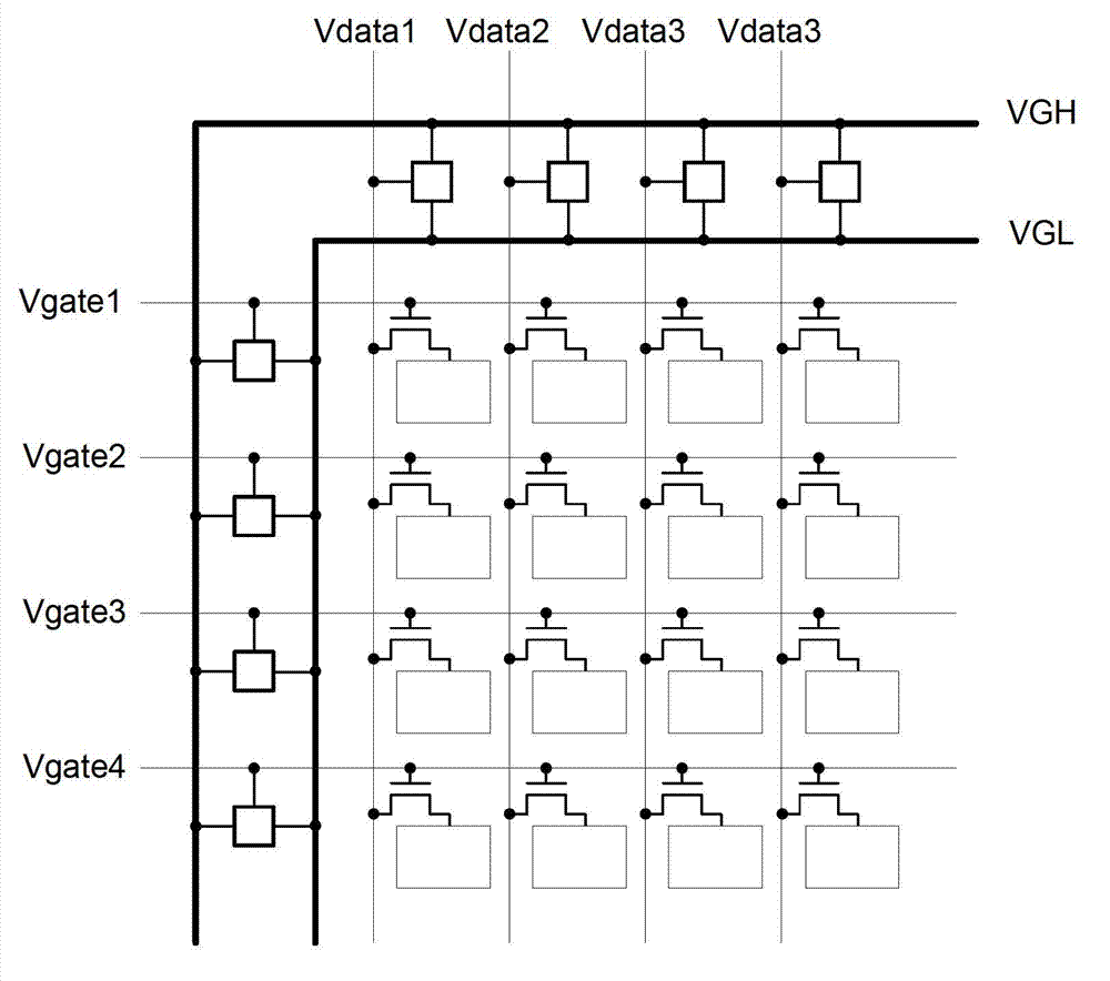
[0069] see Figure 10 , the ESD protection circuit provided by Embodiment 2 of the present invention includes:
[0070] The first thin film transistor 201, its drain is connected to the data signal terminal V data , the source and gate are connected as node Vnet , connected to the drain of the fourth thin film transistor 204;
[0071] The second thin film transistor 202 has its drain connected to the first power voltage terminal VGL, and its source connected to the data signal terminal V data , the gate is connected to the node V net ;
[0072] The third thin film transistor 203, whose drain is connected to the data signal terminal V data , the source is connected to the second power voltage terminal VGH, and the gate is connected to the third power voltage terminal VGH2;
[0073] The source and gate of the fourth thin film transistor 204 are connected to the second power voltage terminal VGH;
[0074] The bootstrap capacitor C2 is located at node V net and data signal ...
PUM
| Property | Measurement | Unit |
|---|---|---|
| current | aaaaa | aaaaa |
Abstract
Description
Claims
Application Information
 - R&D Engineer
- R&D Manager
- IP Professional
- Industry Leading Data Capabilities
- Powerful AI technology
- Patent DNA Extraction
Browse by: Latest US Patents, China's latest patents, Technical Efficacy Thesaurus, Application Domain, Technology Topic, Popular Technical Reports.
© 2024 PatSnap. All rights reserved.Legal|Privacy policy|Modern Slavery Act Transparency Statement|Sitemap|About US| Contact US: help@patsnap.com