Infrared image sensor and forming method thereof

An infrared image and sensor technology, applied in the field of semiconductors, can solve the problems of complex infrared image sensor formation methods, incompatibility of semiconductor processes, etc.

Active Publication Date: 2013-03-20
ZHEJIANG JUEXIN MICROELECTRONICS CO LTD
View PDF5 Cites 21 Cited by
  • Summary
  • Abstract
  • Description
  • Claims
  • Application Information

AI Technical Summary

Problems solved by technology

[0003] However, the formation process of the existing infrared image sensor is a standard semiconductor process, and the above-mentioned packaging

Method used


Image

  • Infrared image sensor and forming method thereof
  • Infrared image sensor and forming method thereof
  • Infrared image sensor and forming method thereof

Examples


Embodiment Construction

[0057] In order to make the above objects, features and advantages of the present invention more comprehensible, specific implementations of the present invention will be described in detail below in conjunction with the accompanying drawings.

[0058] In the following description, specific details are set forth in order to provide a thorough understanding of the present invention. However, the present invention can be implemented in many other ways than those described here, and those skilled in the art can make similar extensions without departing from the connotation of the present invention. Accordingly, the present invention is not limited to the specific embodiments disclosed below.

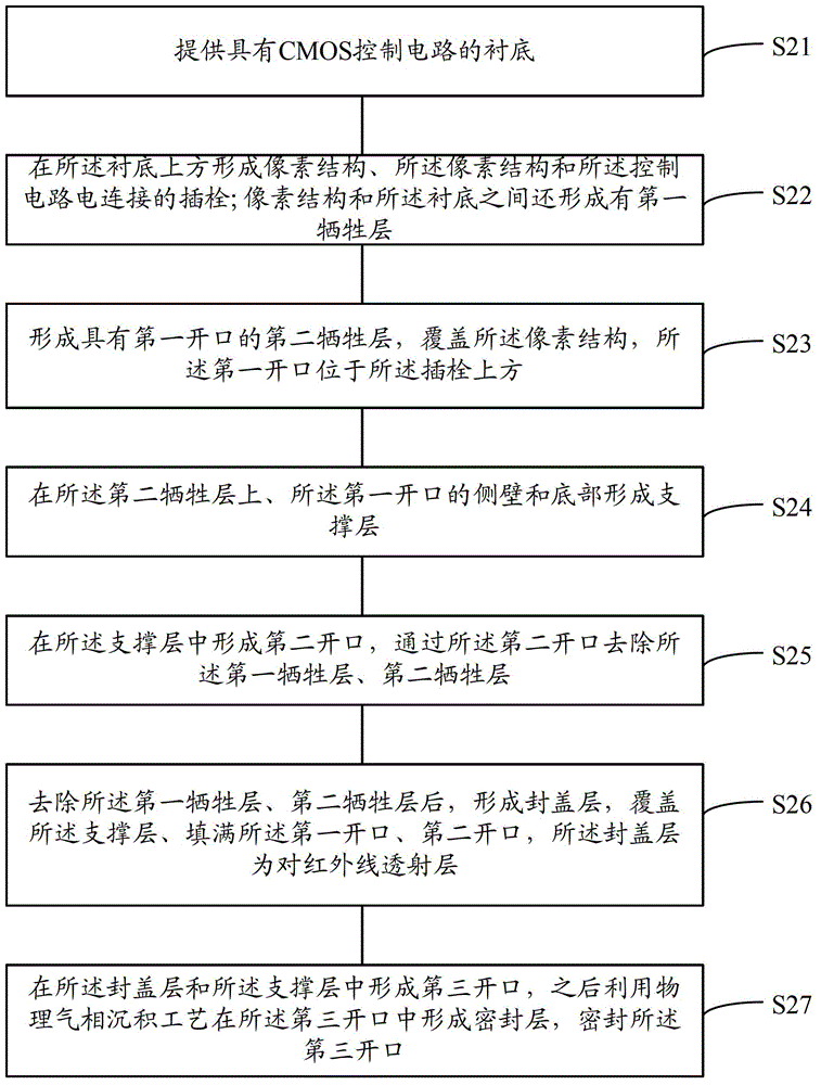
[0059] figure 2 For the flow chart of forming an infrared image sensor in a specific embodiment of the present invention, refer to figure 2 , the method for forming an infrared image sensor according to a specific embodiment of the present invention includes:

[0060] Step S21, providi...


PUM


Abstract

The invention discloses an infrared image sensor and a forming method thereof. The method comprises the steps of providing a substrate with a CMOS (Complementary Metal-Oxide-Semiconductor Transistor) control circuit, forming a pixel structure and a plug for electrically connecting the pixel structure with the control circuit on the substrate, also forming a first sacrifice layer between the pixel structure and the substrate, forming a second sacrifice layer with a first opening and covering the second sacrifice layer on the pixel structure, with the first opening being above the plug, forming a supporting layer on the second sacrifice layer on the side wall and the bottom of the first opening, forming a second opening in the supporting layer, removing the first sacrifice layer and the second sacrifice layer through the second opening, forming a covering layer which is a transmission layer for infrared ray after the first sacrifice layer and the second sacrifice layer are removed, covering the covering layer on the supporting layer, packing the first opening and the second opening, forming a third opening between the covering layer and the supporting layer, and forming a sealing layer in the third opening through a physical vapor deposition technology, so as to seal the third opening. The covering technology in the technical scheme is compatible with the traditional semiconductor technology.

Description

technical field [0001] The invention relates to the technical field of semiconductors, in particular to an infrared image sensor and a forming method thereof. Background technique [0002] Existing infrared image sensors require a separate packaging process. figure 1 It is a schematic diagram of the existing infrared image sensor package structure, refer to figure 1 , after forming the infrared image sensor 10, the infrared image sensor 10 is placed on the metal base 21, and then a temperature control component (not shown) is set on the infrared image sensor 10; The opening on 21 is closed, and then, after the metal base is evacuated, the metal base is sealed, so as to realize the packaging process of the infrared image sensor. [0003] However, the existing infrared image sensor is formed by a standard semiconductor process, and the above-mentioned packaging process is not compatible with the semiconductor process. [0004] In addition, the existing methods for forming i...

Claims


Application Information

Patent Timeline
IPC IPC(8): H01L27/146
Inventor 毛剑宏唐德明张镭
Owner ZHEJIANG JUEXIN MICROELECTRONICS CO LTD
Why Eureka
Try Eureka