Cu-Ni-Si copper alloy plate with excellent deep-draw characteristics and production method thereof

A cu-ni-si, copper alloy plate technology, applied in the direction of metal/alloy conductor, cable/conductor manufacturing, conductive material, etc., can solve the obstacle of raw material application, poor balance of heat-resistant peeling resistance of deep-drawing processable solder, Problems such as insufficient machinability of copper-nickel-silicon alloys

Active Publication Date: 2014-09-03
MITSUBISHI SHINDOH CO LTD
View PDF5 Cites 0 Cited by
  • Summary
  • Abstract
  • Description
  • Claims
  • Application Information

AI Technical Summary

Problems solved by technology

[0012] Most of the conventional Cu-Ni-Si-based copper-nickel-silicon alloys have insufficient deep drawing workability. In addition, the balance between deep drawing workability, solder heat peeling resistance, and elastic limit value is not good. Obstacles in the application of raw materials for electronic components in harsh environments with high temperature and high vibration for a long time

Method used


Image

  • Cu-Ni-Si copper alloy plate with excellent deep-draw characteristics and production method thereof
  • Cu-Ni-Si copper alloy plate with excellent deep-draw characteristics and production method thereof
  • Cu-Ni-Si copper alloy plate with excellent deep-draw characteristics and production method thereof

Examples


Embodiment

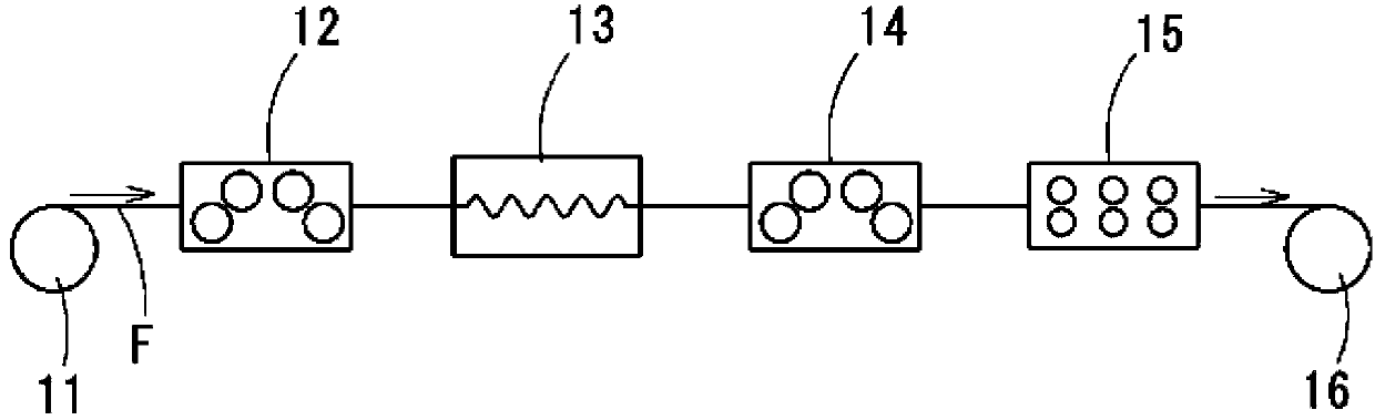
[0088] Materials were prepared so as to have the components shown in Table 1, melted in a low-frequency melting furnace with a reducing atmosphere, and then cast to manufacture a copper alloy ingot with a size of 80 mm in thickness, 200 mm in width, and 800 mm in length. After heating this copper alloy ingot to 900-980 degreeC, the hot-rolled plate of thickness 11mm was formed by hot rolling, and after water-cooling this hot-rolled plate, 0.5 mm flat cutting was performed on both surfaces. Next, cold rolling was performed at a rolling ratio of 87% to produce a cold-rolled sheet with a thickness of 1.3 mm, and continuous annealing was carried out at 710 to 750° C. for 7 to 15 seconds, followed by pickling and surface grinding, and further, Cold rolling was carried out at a rolling ratio of 77% to produce a cold-rolled sheet with a thickness of 0.3 mm.

[0089] After the cold-rolled sheet was kept at 710-780°C for 7-15 seconds, it was rapidly cooled to implement solution treatme...


PUM

PropertyMeasurementUnit
elasticityaaaaaaaaaa
elastic limitaaaaaaaaaa

Abstract

Provided are a Cu-Ni-Si-based copper alloy which has balanced characteristics of deep drawing workability, plating resistance to heat separation and spring bending elastic limit, particularly has an excellent deep drawing workability, and is used in electrical and electronic members, and a method of manufacturing the same. The Cu-Ni-Si-based copper alloy plate contains 1.0 mass% to 3.0 mass% of Ni, and Si at a concentration of 1 / 6 to 1 / 4 of the mass% concentration of Ni with a remainder of Cu and inevitable impurities, in which, when the average value of the aspect ratio (the minor axis of crystal grains / the major axis of crystal grains) of each crystal grains in an alloy structure is 0.4 to 0.6, the average value of GOS in the all crystal grains, which is measured through an EBSD method using a scanning electron microscope equipped with an electron backscatter diffraction image system, is 1.2° to 1.5°, and the ratio (LÃ / L) of the total special grain boundary length LÃ of special grain boundaries to the total grain boundary length L of crystal grain boundaries is 60% to 70%, the spring bending elastic limit becomes 450 N / mm 2 to 600 N / mm 2 , the solder resistance to heat separation is favorable and deep drawing workability is excellent at 150°C for 1000 hours.

Description

technical field [0001] The present invention relates to a Cu-Ni-Si-based copper alloy that has a balance between deep drawability, solder heat peeling resistance, and elastic limit value, and in particular has excellent deep drawability and is suitable for use in electric and electronic components panels and methods of manufacture. Background technique [0002] In recent years, with the thinner and lighter electronic equipment, the miniaturization and thinner of terminals, connectors, etc. have also been developed. Therefore, strength and bending workability are required for them, and they can replace the conventional solid solution such as phosphor bronze or brass. Reinforced copper alloys, copper-nickel-silicon (Cu-Ni-Si-based) alloys, beryllium copper, and titanium copper are in increasing demand for precipitation-strengthened copper alloys. [0003] Among them, copper-nickel-silicon alloy is an alloy in which the solid solution limit of nickel-silicon compound to copper...

Claims


Application Information

Patent Timeline
Patent Type & Authority Patents(China)
IPC IPC(8): C22C9/06C22C9/04C22F1/08H01B1/02H01B13/00C22F1/00
CPCC22C9/06H01B1/026C22C9/10C22C9/04C22F1/00C22F1/08
Inventor 樱井健阿部良雄斋藤晃龟山嘉裕
Owner MITSUBISHI SHINDOH CO LTD
Why Eureka
Try Eureka