High-speed interface and low-speed interface switching circuit and method based on FPGA (Field Programmable Gate Array)

A technology of interface conversion and high-speed interface, which is used in electrical digital data processing, instruments, etc., and can solve problems such as data rate and interface protocol mismatch.

Inactive Publication Date: 2013-03-27
INST OF SEMICONDUCTORS - CHINESE ACAD OF SCI
View PDF5 Cites 21 Cited by
  • Summary
  • Abstract
  • Description
  • Claims
  • Application Information

AI Technical Summary

Problems solved by technology

[0003] The purpose of the present invention is to provide a high-speed interface and low-speed interface conversion circuit and method based on F

Method used


Image

  • High-speed interface and low-speed interface switching circuit and method based on FPGA (Field Programmable Gate Array)
  • High-speed interface and low-speed interface switching circuit and method based on FPGA (Field Programmable Gate Array)
  • High-speed interface and low-speed interface switching circuit and method based on FPGA (Field Programmable Gate Array)

Examples


Embodiment Construction

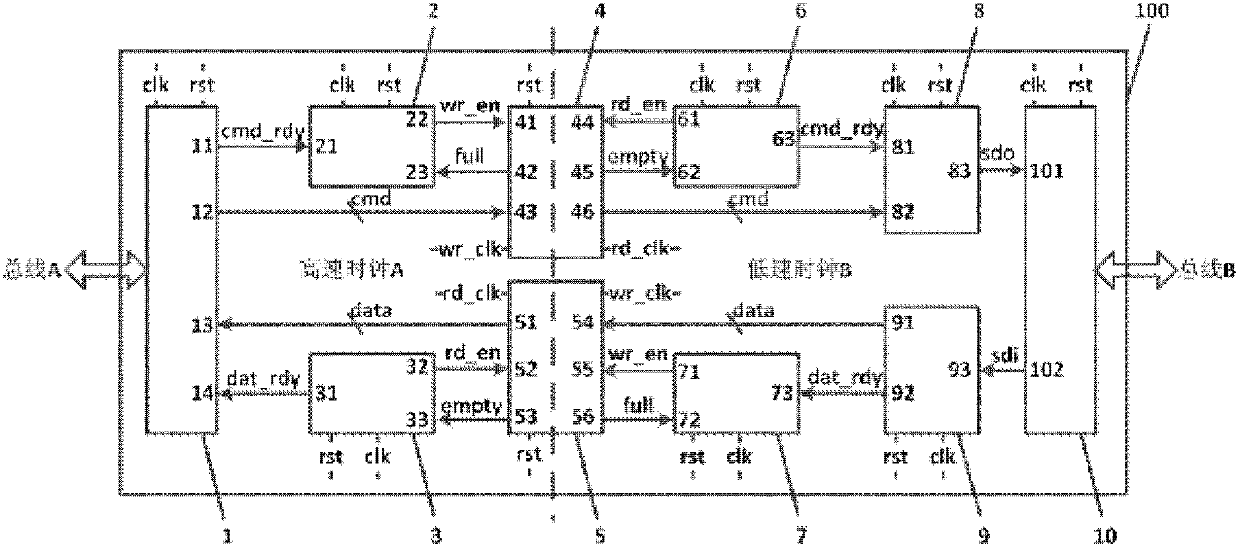
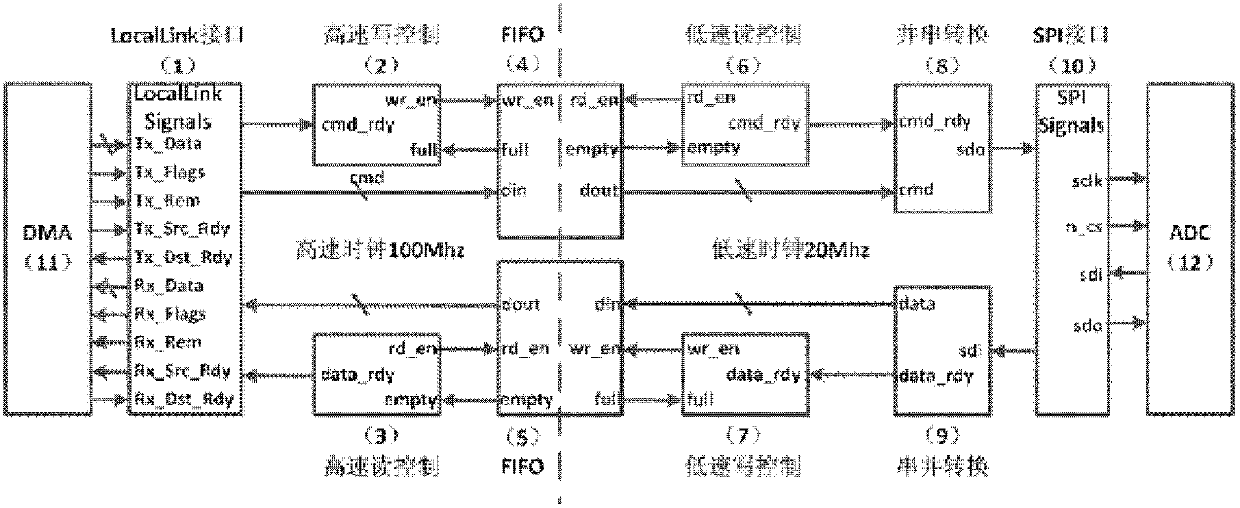
[0026] see figure 1 as shown, figure 1 It is a structural schematic diagram of the conversion circuit provided by the present invention. The conversion circuit 100 includes a high-speed parallel interface module 1, a high-speed write control module 2, a high-speed read control module 3, a first data cache FIFO read-write module 4, and a second data cache FIFO read-write module. Module 5 , low-speed read control module 6 , low-speed write control module 7 , parallel-to-serial conversion module 8 , serial-to-parallel conversion module 9 and low-speed serial interface module 10 . Among them, the high-speed parallel interface module 1 defines a set of protocol-independent control signals according to the characteristics of the parallel bus A to realize variable-length data packet transmission and data flow control; the high-speed write control module 2 is used to control the first data cache FIFO read-write module 4 of the data writing process; the high-speed read control module ...


PUM


Abstract

The invention provides a high-speed interface and low-speed interface switching circuit and method based on an FPGA (Field Programmable Gate Array). The high-speed interface and low-speed interface switching circuit based on the FPGA comprises a high-speed parallel interface module, a high-speed writing control module, a high-speed reading control module, a first data caching FIFO (First In First Out) reading-writing module, a second data caching FIFO reading-writing module, a low-speed reading control module, a low-speed writing control module, a parallel-series switching module, a series-parallel switching module and a low-speed serial interface module. According to the high-speed interface and low-speed interface switching circuit and method based on the FPGA disclosed by the invention, the problem that data rates and interface protocols of a high-speed parallel interface and a low-speed serial interface are not matched in an embedded system can be solved, and meanwhile, full-duplex communication can be realized; and when an Xilinx Virtex-5 series FPGA is adopted, occupied logic resources are few and system integration is easy to realize.

Description

technical field [0001] The invention relates to a conversion circuit and method between different interface buses and different clock domains in a digital circuit system, in particular to a high-speed parallel interface and low-speed serial interface conversion circuit and method based on a field programmable gate array (FPGA). Background technique [0002] Reliable transmission of a large amount of data between different interface buses and different clock domains in digital circuit systems has always been a key issue in digital circuit design; in order to achieve reliable exchange of data between different interface buses and different clock domains, avoid The metastable problem caused by the interface conversion circuit is essential. At present, there are various types of special-purpose interface conversion chips on the market, but the special-purpose interface conversion chips cannot be reconfigured, have a single structure, and have poor flexibility. With the rapid de...

Claims


Application Information

Patent Timeline
IPC IPC(8): G06F13/40
Inventor 陈弘达黄莉张旭
Owner INST OF SEMICONDUCTORS - CHINESE ACAD OF SCI
Why Eureka
Try Eureka