

Metamaterial and metamaterial design method
A design method and metamaterial technology, applied in the field of metamaterials, can solve unrealizable and difficult problems
- Summary
- Abstract
- Description
- Claims
- Application Information
AI Technical Summary
Problems solved by technology
Method used
Image

Examples
Embodiment Construction
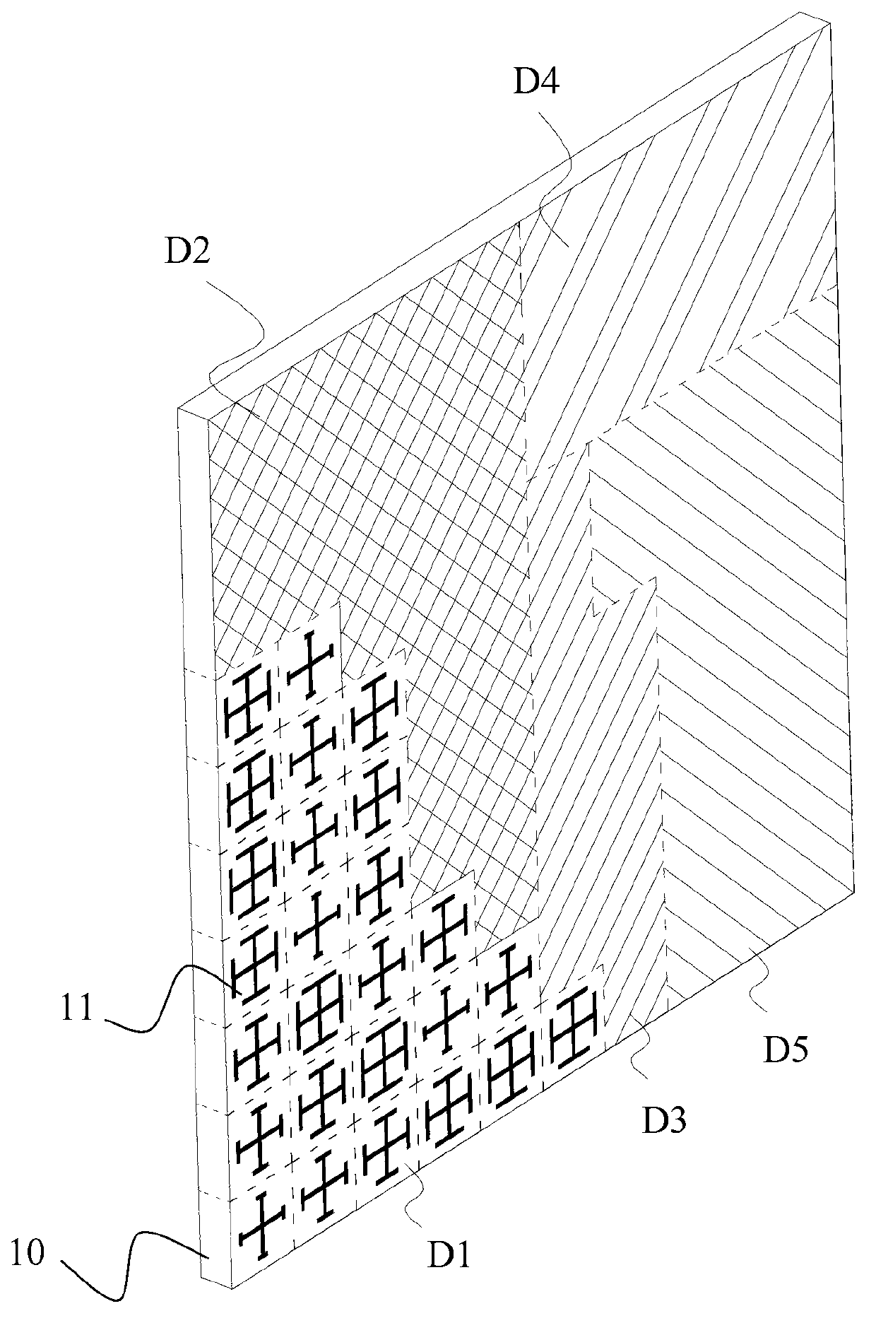
[0064] Please refer to figure 1 , figure 1 It is a schematic diagram of a three-dimensional structure in a preferred embodiment of the metamaterial of the present invention. figure 1 Among them, the metamaterial includes a substrate 10 and a plurality of artificial microstructures 11 arranged on the surface of the substrate 10. The metamaterial includes multiple electromagnetic regions D1, D2, D3, D4, and D5. figure 1 In the electromagnetic region D1, a plurality of artificial microstructures 11 are arranged, and other electromagnetic regions are filled with different filling patterns to show distinction. However, it can be seen that there are also a plurality of artificial microstructures in other electromagnetic regions. Each electromagnetic area corresponds to one or more electromagnetic parameter ranges of electromagnetic waves incident into the electromagnetic area.
[0065] figure 1 In this case, the surface of the substrate 10 is flat. The method for providing artificial m...
PUM
 Abstract
Description
Claims
Application Information