Optical device coupling device

A technology of coupling device and optical device, which is applied to the coupling of optical waveguides, etc., can solve the problems of unqualified product performance, displacement, and inability to guarantee product electrical performance parameters, and achieve the effect of ensuring accuracy and coupling speed.

Inactive Publication Date: 2013-04-03
绍兴飞泰光电技术有限公司
View PDF7 Cites 1 Cited by
  • Summary
  • Abstract
  • Description
  • Claims
  • Application Information

AI Technical Summary

Problems solved by technology

[0006] The receiving end coupling method of traditional optical devices basically adopts a single fixture coupling method. Due to the different positions of the die clamping each time, in addition to adjusting the X / Y two directions for each coupling product, the Z axis direction also needs to be adjusted, so that The coupling time is extended; after the coupling is completed, the UV glue is baked by the person holding the UV light source. The operator can couple the next product only after the glue is baked, which is a waste of man-hours, and the UV light protection effect is not good.
When the glue is finished and the material is returned, the operator directly pulls out the product manually, which may easily cause the coupling position pre-fixed with UV glue to move, resulting in unqualified product performance
The electrical performance parameters of the coupling are also the amplitude of the single-coupling differential output signal or the responsivity of the single-coupling PD / APD, which cannot guarantee that all electrical performance parameters of the product are qualified, causing hidden dangers in product performance

Method used


Image

  • Optical device coupling device
  • Optical device coupling device
  • Optical device coupling device

Examples


Embodiment Construction

[0029] The present invention will be further described below in conjunction with the accompanying drawings and specific embodiments.

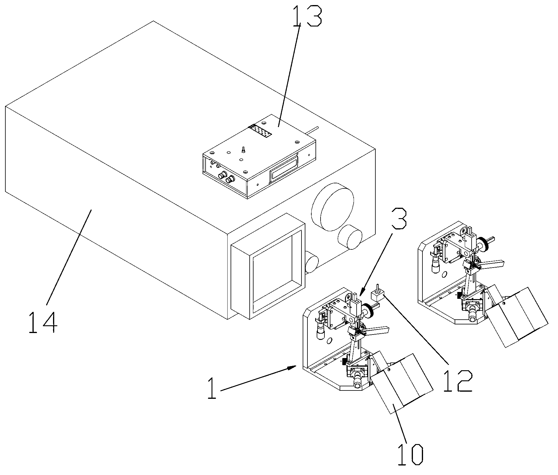
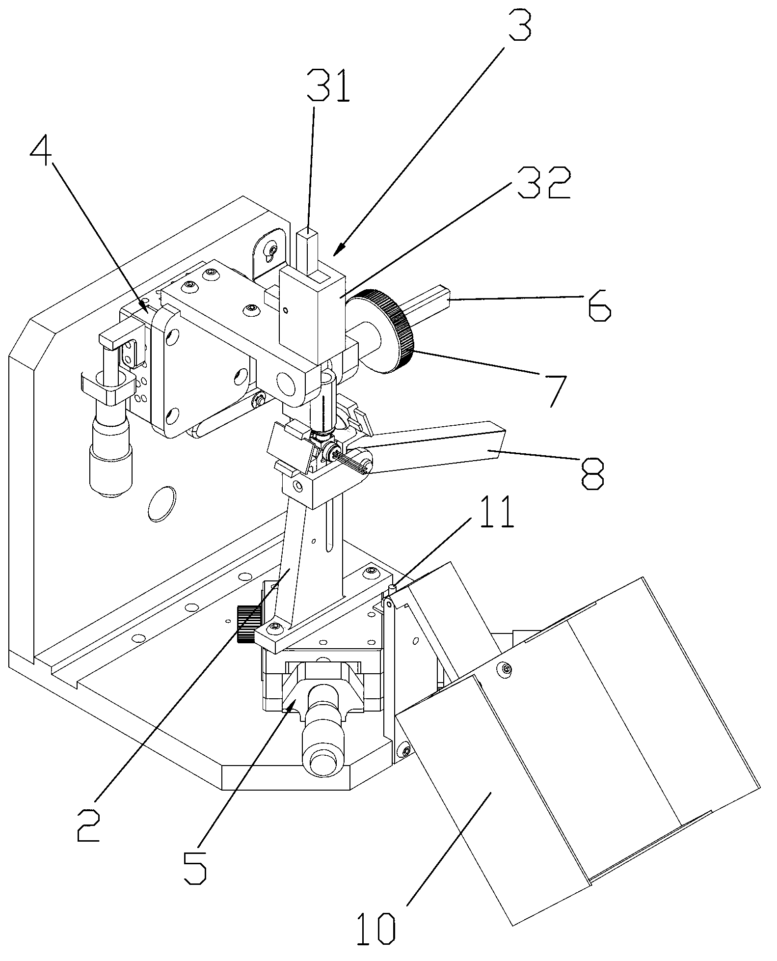
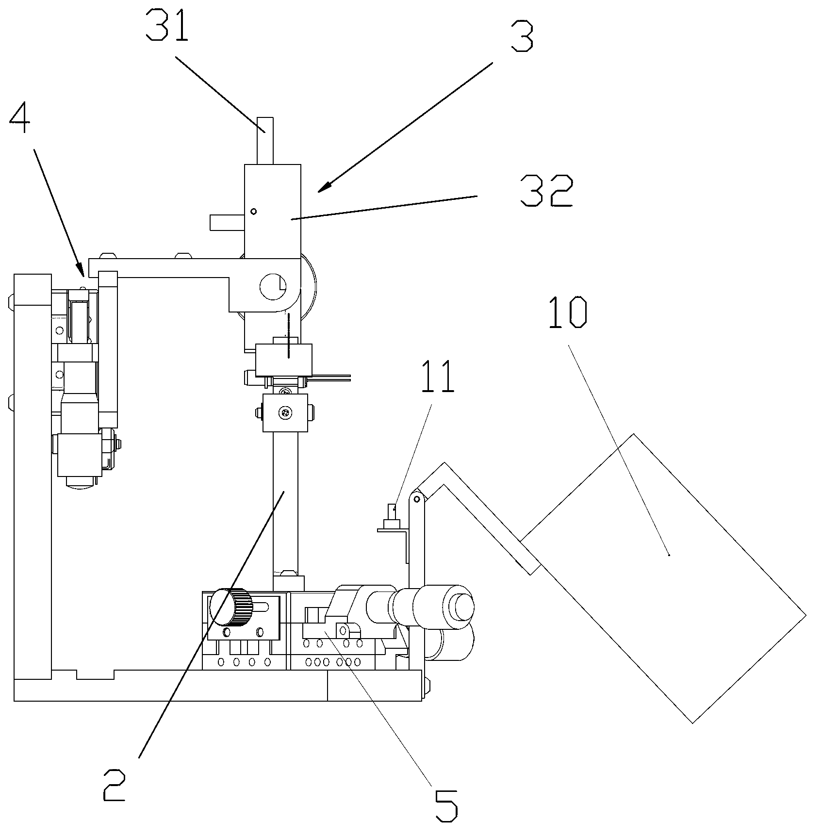
[0030] As shown in the figure, an optical device coupling device disclosed by the present invention includes two coupling fixtures 1, and the coupling fixture 1 includes a base clamp 2, a material return device 3, a fine-tuning frame A4, and a fine-tuning frame B5, through which the fine-tuning frame A4 and The fine-tuning frame B5 adjusts the positions of the stripping device 3 and the base clamp 2, and couples the response voltage signal to dispensing and baking the glue to fix it when it is enlarged.

[0031] The base clamp 2 is arranged on the fine-tuning frame B5, and is used for clamping the semi-finished base. The stripping device 3 is arranged on the fine-tuning frame A4, and comprises stripping bar 31, socket block 32, and stripping bar 31 can move in socket block 32, and the bottom of stripping bar 31 is provided with tube core 91 hol...


PUM


Abstract

The invention relates to the field of optical devices, in particular to an optical device coupling device which comprises a coupling clamp. The coupling clamp comprises a base clamp, a material returning device, a fine adjustment frame A and a fine adjustment frame B. The base clamp is arranged on the fine adjustment frame B, the material returning device is arranged on the fine adjustment frame A, a tube core is clamped through the material returning device, a base is clamped through the base clamp, the material returning device and the base clamp are adjusted through the fine adjustment frame A and the fine adjustment frame B, and glue dispensing and glue baking fixing are performed when response voltage signals are coupled to be large. After the technical scheme is adopted, precision of an optical device in coupling is improved, coupling efficiency is improved, production efficiency is improved, product performance is guaranteed, and the production cost of the device is also reduced simultaneously.

Description

[0001] technical field [0002] [0003] The invention relates to the field of optical devices, in particular to an optical device coupling device. [0004] Background technique [0005] In recent years, the domestic optical communication industry has developed rapidly, and the market demand for optical devices has continued to increase. The problems of production capacity, production cost, and product stability have become the most urgent problems for optical device manufacturers to solve. (Optical devices are mainly divided into: ROSA single-receiving components, TOSA single-transmitting components, BOSA single-fiber transceiver components, etc.) [0006] The receiving end coupling method of traditional optical devices basically adopts a single fixture coupling method. Due to the different positions of the die clamping each time, in addition to adjusting the X / Y two directions for each coupling product, the Z axis direction also needs to be adjusted, so that The couplin...

Claims


Application Information

Patent Timeline
Patent Type & Authority Applications(China)
IPC IPC(8): G02B6/42
Inventor 温永阔杨圣王苗庆王珑锟
Owner 绍兴飞泰光电技术有限公司
Why Eureka
Try Eureka