Supercharge Your Innovation With Domain-Expert AI Agents!

Semiconductor component and method for producing a semiconductor component

A technology of semiconductors and optoelectronic semiconductors, applied in semiconductor devices, electrical components, circuits, etc., can solve problems such as radiation efficiency decline and absorption loss

Active Publication Date: 2013-04-03
OSRAM OPTO SEMICONDUCTORS GMBH
View PDF8 Cites 6 Cited by
  • Summary
  • Abstract
  • Description
  • Claims
  • Application Information

AI Technical Summary

Problems solved by technology

[0004] In radiation-emitting semiconductor components, for example in components with light-emitting diode chips for generating radiation, parts of the radiation scattered back, for example on lamp housings, can be absorbed in the component, as a result of which the overall efficiency of radiation generation is reduced
[0005] Especially in devices where the semiconductor chip is mounted directly on a flat carrier, significant losses can result due to carrier absorption

Method used


Image

  • Semiconductor component and method for producing a semiconductor component
  • Semiconductor component and method for producing a semiconductor component
  • Semiconductor component and method for producing a semiconductor component

Examples


Embodiment Construction

[0041] The same, the same type or the same function elements are provided with the same reference signs in the figures.

[0042] The figure and the size ratio of the elements shown in the figure to each other cannot be regarded as to scale. On the contrary, for better visibility and / or for better understanding, individual elements, especially layer thicknesses, can be exaggerated.

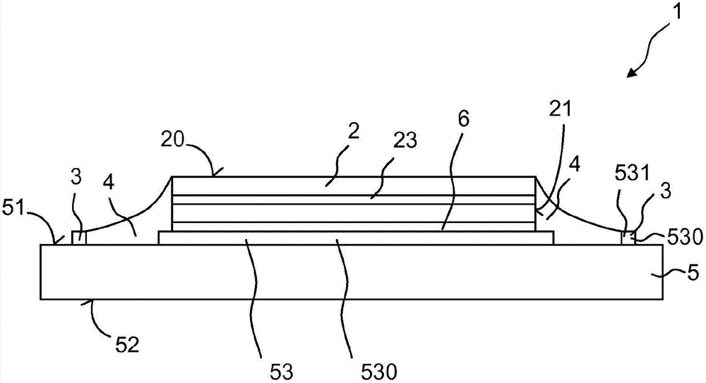
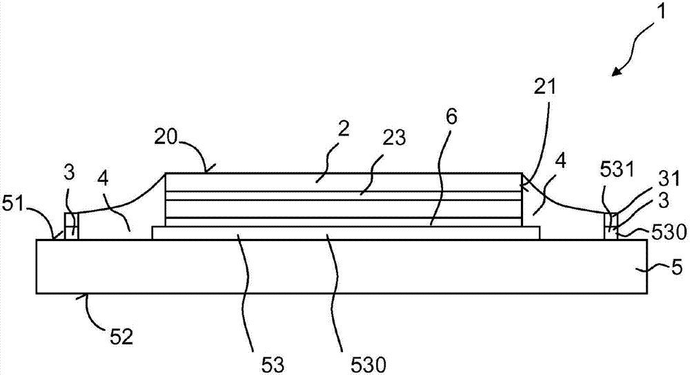
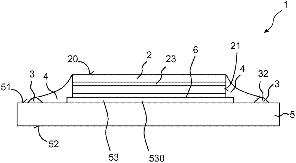
[0043] in figure 1 The first embodiment of the semiconductor device is schematically shown in a cross-sectional view in FIG. The semiconductor component 1 has a semiconductor chip 2 which is arranged on the connection surface 53 of the connection carrier 5. The semiconductor chip is fixed on the connection surface by means of the connection layer 6. Therefore, the semiconductor chip is fixed on the flat connection carrier in a flat arrangement without packaging.

[0044] The semiconductor chip 2 is configured as a light-emitting diode semiconductor chip, in which an active region 23 of the semiconduct...


PUM


Abstract

The invention relates to a semiconductor component (1) comprising at least one optoelectronic semiconductor chip (2) and a connecting carrier (5) having a connecting surface (53) on which the semiconductor chip (2) is disposed. A reflective coating (4) and a limiting structure (3) are formed on the connecting carrier (5), wherein the limiting structure (3) at least partially encloses the semiconductor chip (2) in the lateral direction, and the reflective coating (4) at least partially extends in the lateral direction between a side surface (21) of the semiconductor chip and the limiting structure (3). The invention further relates to a method for producing a semiconductor component.

Description

Technical field [0001] The application relates to a semiconductor device and a method for manufacturing the semiconductor device. [0002] Cross-reference of related applications [0003] This application claims the priority of German patent application 102010031945.7, the disclosure of which is hereby incorporated by reference. Background technique [0004] In a radiation-emitting semiconductor device, such as a device having a light-emitting diode chip for generating radiation, for example, the portion of the radiation scattered back on the lamp housing can be absorbed in the device, thereby reducing the efficiency of radiation generation as a whole . [0005] Especially in a device in which the semiconductor chip is directly mounted on a flat carrier, a large loss can be caused due to the absorption of the carrier. Summary of the invention [0006] The purpose is to propose a semiconductor device in which absorption loss is reduced. In addition, a method for manufacturing such se...

Claims


Application Information

Patent Timeline
Patent Type & Authority Applications(China)
IPC IPC(8): H01L33/46H01L33/60
CPCH01L31/18H01L33/46H01L2933/0025H01L33/60H01L31/0232H01L33/44H01L33/58
Inventor 西蒙·耶雷比奇埃里克·海涅曼克里斯蒂安·盖特纳阿莱斯·马尔基坦
Owner OSRAM OPTO SEMICONDUCTORS GMBH
Features
  • R&D
  • Intellectual Property
  • Life Sciences
  • Materials
  • Tech Scout
  • Unparalleled Data Quality
  • Higher Quality Content
  • 60% Fewer Hallucinations
Learn More