Electric connector and manufacturing method thereof

A technology for electronic connectors and connecting devices, which is applied in the direction of contact manufacturing, connection, and contact box/base manufacturing, etc., which can solve problems such as damage, small space, and easy breakage of free ends, and achieve low cost, high precision, and Ease of mass production

Inactive Publication Date: 2013-04-10
JIH VEI ELECTRONICS KUSN
View PDF4 Cites 2 Cited by
  • Summary
  • Abstract
  • Description
  • Claims
  • Application Information

AI Technical Summary

Problems solved by technology

Usually, devices such as PCB connectors can be used to splice several PCB boards together, thereby compressing and obtaining a smaller space. The existing connectors have many disadvantages. For example, the electronic components on the PCB have a certain height. When two When PCBs are spliced ​​together, in order to prevent the two opposite electronic components from touching each other, it is usually required that the PCB connector has an ideal height.
However, due to the influence of the existing technology, it is difficult for the height of the PCB connector to reach more than 15mm
Because in the existing process, the remaining part of one side of the section is usually cut before the copper sheet is cut, so that the side of the copper sheet becomes a free end after cutting to form the PIN needle, which limits the length of the PIN needle because the PIN needle is too long , its free end is easily broken or damaged, and it is not convenient for subsequent processing

Method used


Image

  • Electric connector and manufacturing method thereof
  • Electric connector and manufacturing method thereof
  • Electric connector and manufacturing method thereof

Examples


Embodiment Construction

[0027] The present invention will be described in further detail below in conjunction with the accompanying drawings.

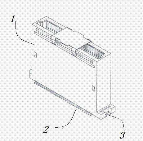
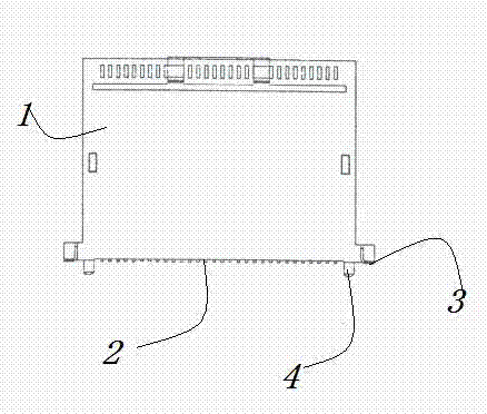
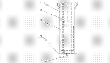
[0028] like figure 1 and figure 2 and image 3 As shown, the electronic connector of the present invention includes a shell 1 with upper and lower openings and two rows of PIN pins 2 arranged inside the shell 1 on the front and rear sides. Greater than 15mm, preferably greater than 22mm, this length can ensure that the relative electronic components have a sufficient distance when splicing PCB boards, and avoid mutual interference between PIN pins 2. The casing 1 is integrally molded by plastic injection molding, which has many advantages such as low cost, high precision, and convenience for large-scale production. One side of the PIN needle 2 is flush with the upper end of the shell 1, and a part of one side protrudes from the lower end of the shell 1, and the protruding part is bent outward. The two PIN needles 2 connected on each side are separated by...


PUM


Abstract

The invention discloses an electric connector and manufacturing method thereof, the electric connector and manufacturing method thereof comprises a shell with opening up and down, two rows of (PIN) pins are arranged on the bilateral sides of the inner portion of the shell, the length of the pins covers at least the up and down height of the shell, the up and down height of the shell is at least taller than 15 millimeters so that ensuring sufficient distance of a relative electric component split joint with a (printed circuit board)PCB board. The manufacturing method of the electric connector and manufacturing method thereof comprises the residue portion connecting the pins together of two ends cross a copper sheet formed by copper sheet blank, the pins are placed into a mould, thereby injection molding forming the shell, bending the pin 2 emerging from the bottom portion of the shell 1, cutting the residue portion of the two ends of the pins. The electric connector and manufacturing method thereof can a free end produced by the pins and limit the length of the pins after placing the chopped-off residue portion into the injection molding.

Description

technical field [0001] The invention relates to a device for connecting two PCB boards and a method for manufacturing the PCB board connecting device. Background technique [0002] PCB (Printed Circuit Board), the Chinese name is printed circuit board, also known as printed circuit board, printed circuit board, is an important electronic component, a support for electronic components, and a provider of electrical connections for electronic components. Because it is made using electronic printing, it is called a "printed" circuit board. [0003] As electronic products become smaller and smaller, PCB boards will also become smaller and smaller. Usually, devices such as PCB connectors can be used to splice several PCB boards together, thereby compressing and obtaining a smaller space. The existing connectors have many disadvantages. For example, the electronic components on the PCB have a certain height. When two When PCBs are spliced ​​together, in order to prevent two oppos...

Claims


Application Information

Patent Timeline
Patent Type & Authority Applications(China)
IPC IPC(8): H01R13/46H01R13/73H01R13/02H01R13/40H01R12/73H01R43/16H01R43/18
Inventor 郭土水江清源
Owner JIH VEI ELECTRONICS KUSN
Why Eureka
Try Eureka