Array substrate and display panel
An array substrate and display area technology, applied in nonlinear optics, instruments, optics, etc., can solve the problems of integrated circuit uniformity differences, defects, and increased display, and achieve the effect of avoiding poor binding uniformity
- Summary
- Abstract
- Description
- Claims
- Application Information
AI Technical Summary
Problems solved by technology
Method used
Image

Examples
Embodiment 1
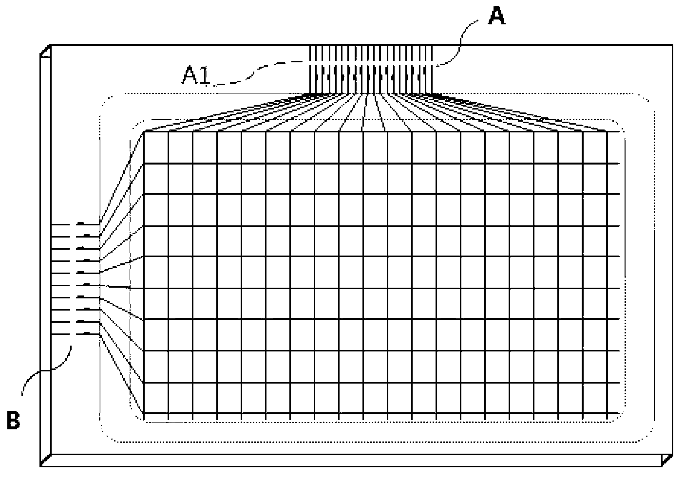
[0031] An array substrate provided in Embodiment 1 of the present invention includes a display area, a non-display area, and a driving circuit, wherein the display area includes a plurality of data lines and a plurality of gate lines, and the non-display area includes The data signal input end of the data line input signal, here you can also refer to the attached figure 1 shown.
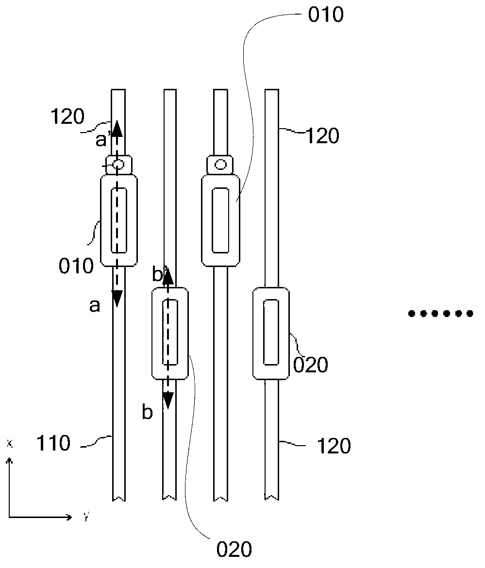
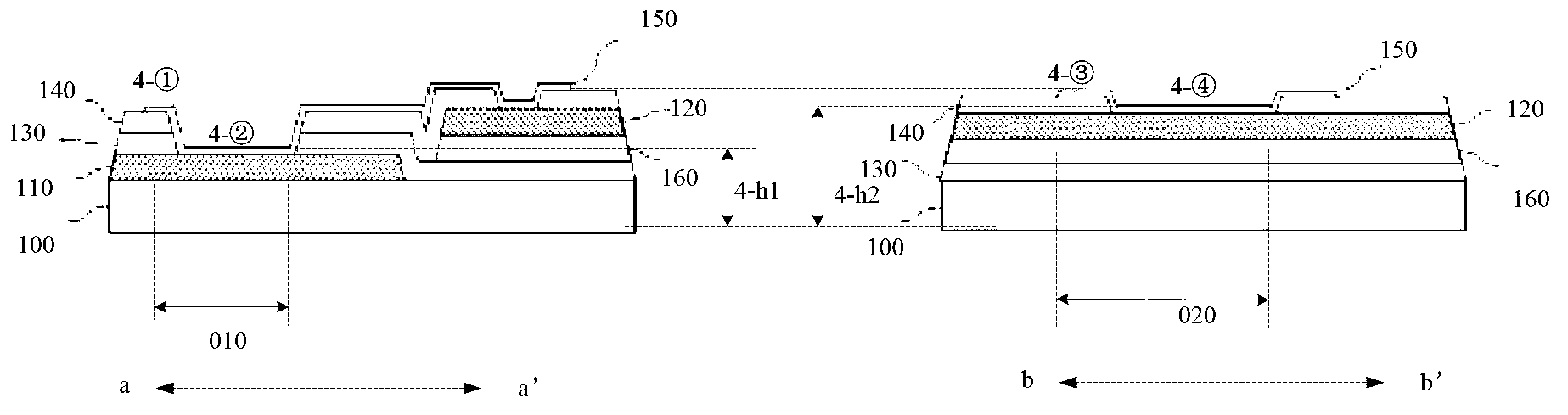
[0032] The data signal input terminal will be described in detail below in conjunction with the accompanying drawings. see Figure 4 , the data signal input terminal includes a plurality of first leads 200 and second leads 300 corresponding to the data lines of the display area and arranged at intervals; wherein the first leads 200 include the same layer as the gate lines of the display area The formed first gate lead 211 and the first data line lead 212 formed on the same layer as the data line in the display area, the first via hole is formed above the first gate lead 211 and the first data line ...
Embodiment 2
[0043] The difference between the array substrate provided in Embodiment 2 of the present invention and the array substrate provided in Embodiment 1 is that the array substrate described in Embodiment 2 is manufactured through five patterning processes, as shown in Figure 7 As shown, there is no active layer between the first insulating layer 130 and the first data line lead 212 and between the first insulating layer 130 and the second data line lead 312 . However, the same as the embodiment, the first conductive layer and the second conductive layer bonded to the driving circuit are made on the same layer, and both have a height of 5-h2, so it is also avoided that the bonding area is caused by a difference in height. The display of is not good.
[0044] Specifically, see Figure 8(a) to Figure 8(e), the preparation method includes:
[0045] On the glass substrate, a pattern including gate lines and each first gate lead 211 is formed by metal deposition, exposure, development...
PUM
 Abstract
Description
Claims
Application Information
PatSnap Eureka turns technology decisions into work you can execute. Powered by our Innovation Knowledge Graph, it runs expert workflows across engineering, life sciences, materials and intellectual property. Get your review-ready output in minutes.


