

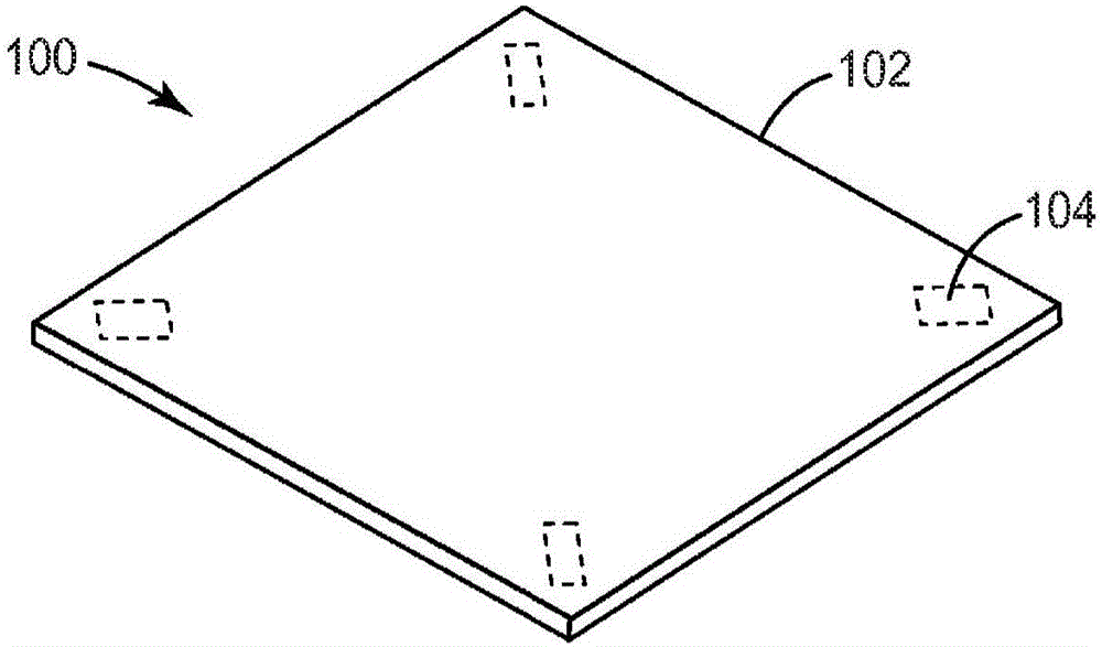
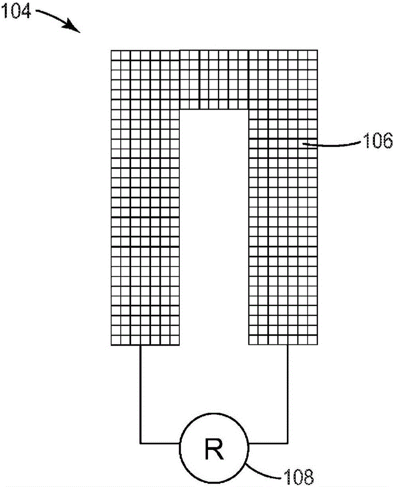
Positioning touch sensor including force measurement
A touch sensor and display technology, applied in the input/output process of instruments, data processing, calculation, etc., can solve the problems of blurred, unsuitable, and limited visibility of the display
- Summary
- Abstract
- Description
- Claims
- Application Information
AI Technical Summary
Problems solved by technology
Method used
Image

Examples
example 1
[0079] Example 1 - Formation of a Display with a Touch Sensor with Piezoresistive Pressure Responsive Material
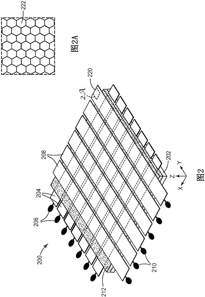
[0080] The first and second patterned substrates prepared above were used to produce a two-layer force-sensing touch sensor comprising a piezoresistive pressure-responsive material. A pressure-responsive material is disposed between the first and second patterned substrates, with the patterned surface of each substrate (having a micropattern of conductive traces) facing the pressure-responsive material. The pressure responsive material is a composite of transparent conductive particles dispersed in a matrix. A film derived from conductive ITO ink in Example 1 of US Patent No. 5,763,091 (Kawata et al.) was used as the pressure responsive material. The film can be coated onto the micropattern of conductive traces of the first patterned substrate. The film is selectively coated onto the substrate surface to cover the first band and the first discontinuous region, b...
example 2
[0082] Example 2 - Formation of Displays with Touch Sensors with Piezoresistive Pressure Responsive Materials .
[0083] The first and second patterned substrates prepared above can be used to produce a two-layer force-sensing touch sensor comprising a piezoresistive pressure-responsive material. A pressure responsive material may be disposed between the first and second patterned substrates, with the patterned surface of each substrate (with the micropattern of conductive traces) facing the pressure responsive material. The pressure-responsive material is a multi-layer sequentially formed of the following material components: i) a first conductive polymer layer; ii) a composite layer of transparent conductive particles dispersed in a matrix; and iii) a second conductive polymer layer. The first conductive polymer layer and the second conductive polymer layer have the same composition and thickness. A film derived from a conductive ITO ink in Example 1 of US Patent No. 5,76...
example 3
[0085] Example 3 - Formation of Displays with Touch Sensors with Piezoresistive Pressure Responsive Materials .
[0086]The first and second patterned substrates prepared above can be used to produce a two-layer force-sensing touch sensor comprising a piezoresistive pressure-responsive material. The pressure-responsive material is included in a multilayer sequentially formed of the following material components: i) a first transparent conductive adhesive layer; ii) a piezoresistive layer; and iii) a second transparent conductive adhesive layer. Banded regions of the first and second patterned substrates are first printed with a transparent conductive adhesive material to form first and second transparent conductive adhesive layers. A transparent conductive adhesive material was prepared according to Example 24 of US Patent Publication No. 2003 / 0114560 (Yang et al.). The transparent conductive adhesive material is printed using inkjet printing, as is known in the art. A non...
PUM
| Property | Measurement | Unit |
|---|---|---|
| width | aaaaa | aaaaa |
| width | aaaaa | aaaaa |
| thickness | aaaaa | aaaaa |
Abstract
Description
Claims
Application Information