Input device
An input device and input component technology, applied in the input/output process of data processing, optics, instruments, etc., can solve problems such as difficult correspondence, and achieve the effects of stable electrical performance and reliable insulation
- Summary
- Abstract
- Description
- Claims
- Application Information
AI Technical Summary
Problems solved by technology
Method used
Image

Examples
no. 1 approach )
[0052]The input device according to the present invention can be applied to a product in which a wiring pattern is formed on a transparent portion such as a transparent input device such as a transparent antenna, a transparent electromagnetic wave shield, or a capacitive or film-type transparent touch panel. Furthermore, the input device of the present invention can be used to form necessary electrodes in a capacitive input device attached to an automobile handle, a capacitive sensor, etc. provided on the surface of a three-dimensional molded product or a three-dimensional decorative molded product. Use for purpose. In addition, "transparent" in this embodiment means having a light transmittance of 50% or more.
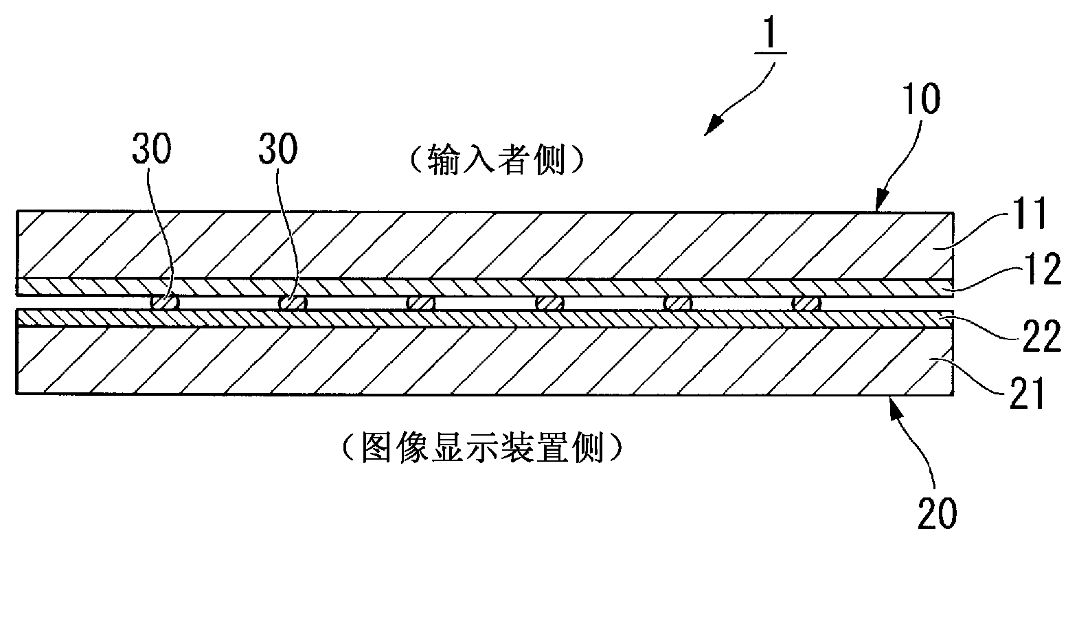
[0053] figure 1 as well as Figure 10 An input member 1 for a film-type touch panel (input device) according to the first embodiment of the present invention is shown. exist Figure 1 ~ Figure 3 Among them, this film type touch panel includes: an input member 1, a...
no. 2 approach )
[0116] Next, refer to Figure 12 to Figure 16 , the input device according to the second embodiment of the present invention will be described. In addition, the same reference numerals are assigned to the same components as those in the above-mentioned embodiment, and description thereof will be omitted.
[0117] The input device according to this embodiment is a capacitive touch panel. Figure 12 An input member 200 for a capacitive touch panel (input device) is shown. This capacitive touch panel includes upper and lower electrodes (transparent conductive films 212 and 222 ) that are capacitively coupled to human body parts H such as fingers via an insulating layer 240 disposed on the side facing the input user. And measure the electrode on the other side to detect the contact condition of the finger.
[0118] like Figure 15 , Figure 16 As shown, the input unit 200 of the electrostatic capacitive touch panel faces one side (input side) along the thickness direction (th...
manufacture example 1
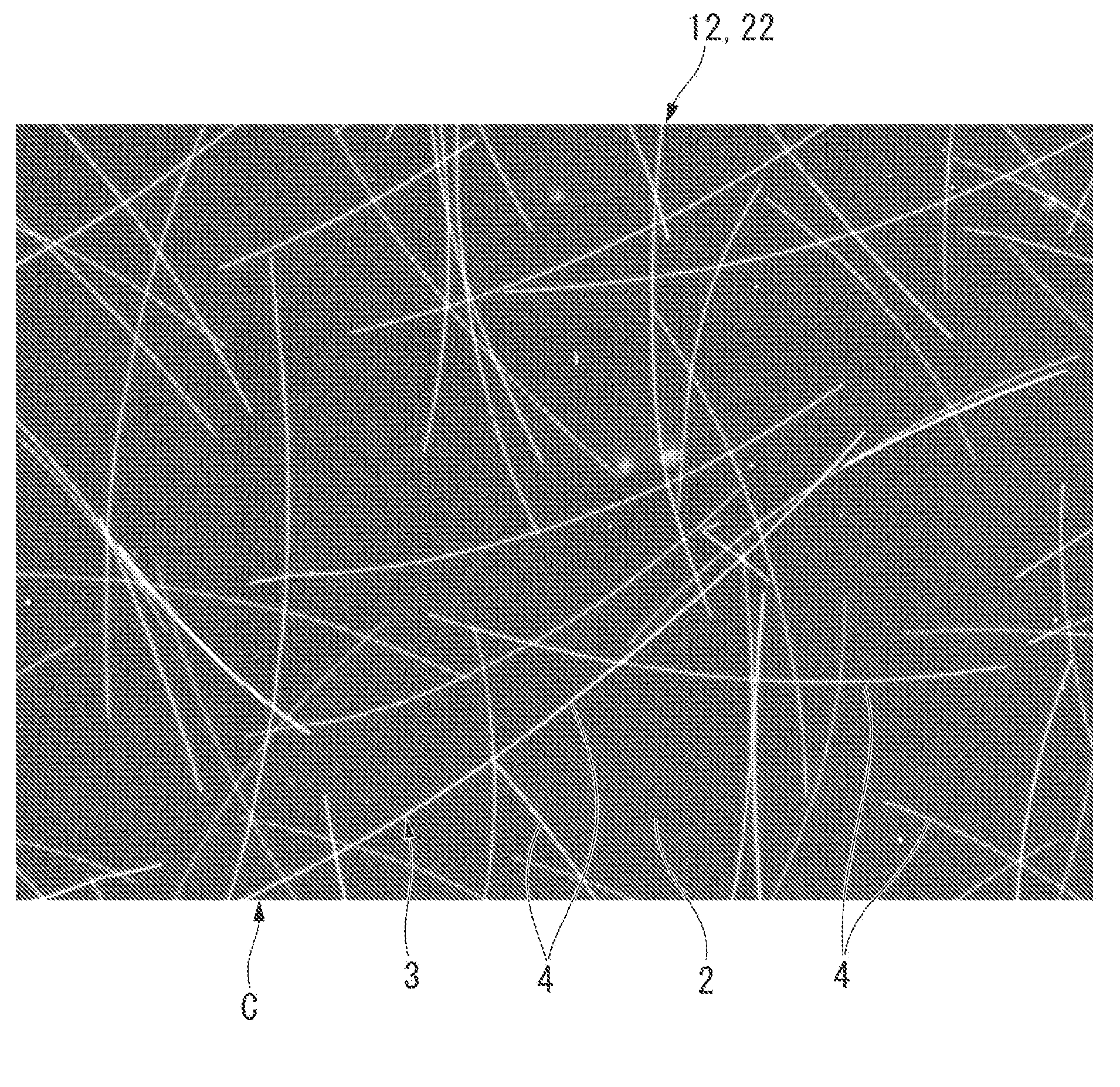
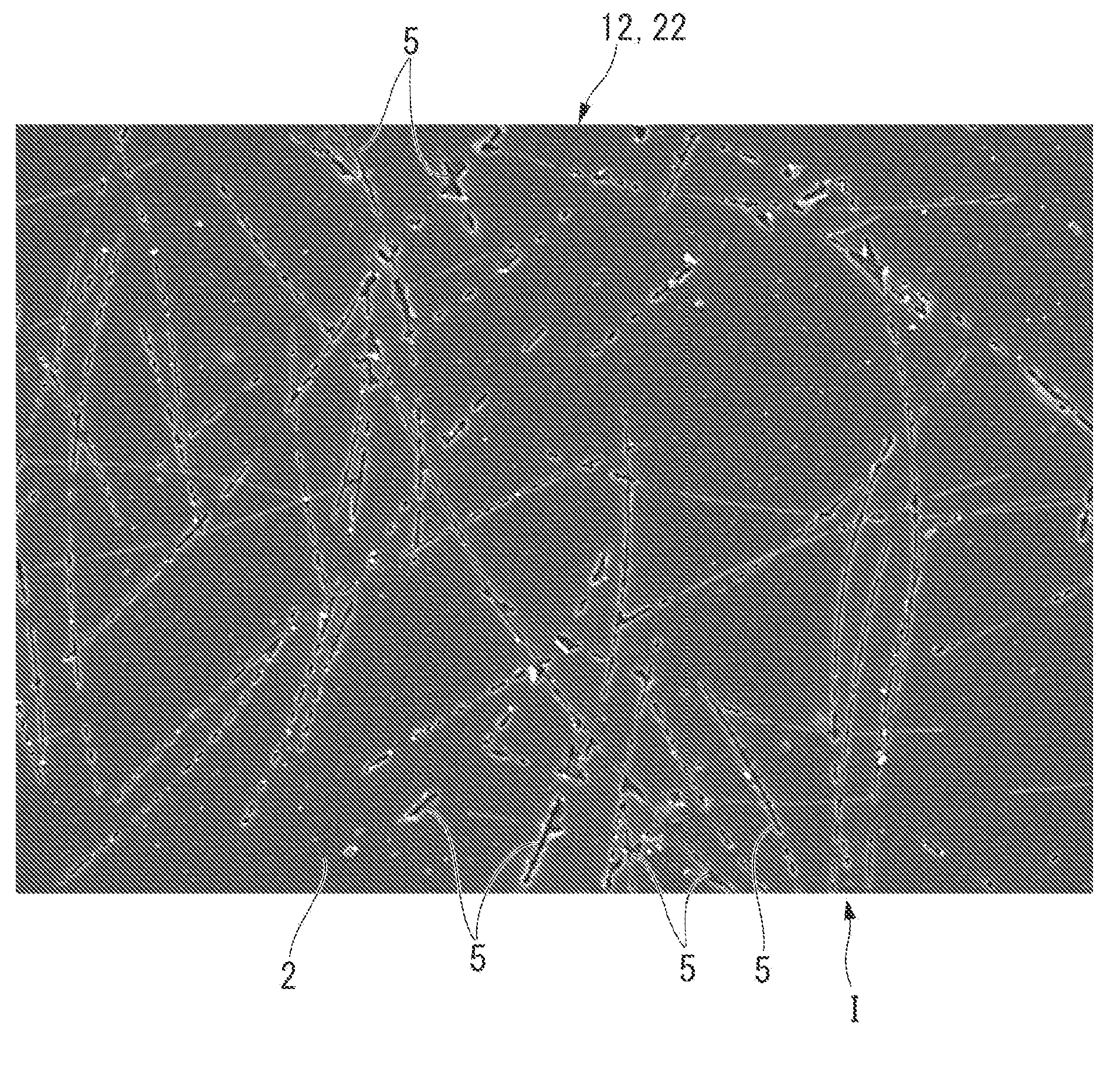
[0139] [Manufacturing example 1] Fabrication of a silver nanowire conductive thin film (conductive substrate) used in an input part of an input device (an example of the present invention)
[0140] After coating and drying Cambrios Ohm (trade name) ink (metal microfiber 4) on transparent polyester (PET) films (insulating substrates 11 and 21) with a thickness of 100 μm, UV-curable Polyester resin ink (transparent substrate 2), drying / ultraviolet treatment to form a conductive two-dimensional network composed of silver fibers (metal ultrafine fibers 4) with a wire diameter of about 50nm and a length of about 15μm on the PET film (Mesh member 3) The friction-resistant transparent conductive layer a ( figure 2 ).
[0141] The surface resistance of the transparent conductive layer a of the silver nanowire conductive film (conductive substrates 10 and 20 ) is 230Ω / □, and the light transmittance is 95%.
[0142] Next, the silver nanowire conductive film was cut and processed into...
PUM
| Property | Measurement | Unit |
|---|---|---|
| Diameter | aaaaa | aaaaa |
| Length | aaaaa | aaaaa |
| Wire diameter | aaaaa | aaaaa |
Abstract
Description
Claims
Application Information
 - R&D Engineer
- R&D Manager
- IP Professional
- Industry Leading Data Capabilities
- Powerful AI technology
- Patent DNA Extraction
Browse by: Latest US Patents, China's latest patents, Technical Efficacy Thesaurus, Application Domain, Technology Topic.
© 2024 PatSnap. All rights reserved.Legal|Privacy policy|Modern Slavery Act Transparency Statement|Sitemap