
One-step forming method of inner layer circuit of multi-layer flexible circuit board

A flexible circuit board and inner-layer circuit technology, which is applied in the direction of multi-layer circuit manufacturing, etc., can solve the problems of low product qualification rate, expansion and contraction of flexible boards, and false dry film on inner-layer flexible boards.

Active Publication Date: 2016-04-06
SHENZHEN XINYU TENGYUE ELECTRONICS
View PDF5 Cites 0 Cited by
  • Summary
  • Abstract
  • Description
  • Claims
  • Application Information

AI Technical Summary

Problems solved by technology

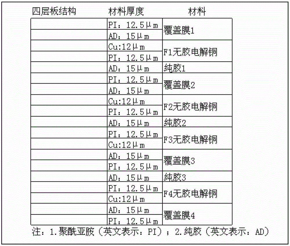
[0002] In the existing technology for producing flexible circuit boards, the commonly used production process for the inner layer circuit of four to eight layer boards is: the inner layer base material is stacked layer by layer and then pressed and solidified, and then the inner layer circuit is made. This method leads to After lamination of the soft board, the height of the glued area and the non-adhesive area are obvious, and the dry film of the inner soft board is not solid, and the soft board is expanded and shrunk after repeated pressing of the inner cover film, which eventually leads to The qualified rate of the product is low, and the production process of the prior art is long and the productivity is low

Method used


Image

  • One-step forming method of inner layer circuit of multi-layer flexible circuit board
  • One-step forming method of inner layer circuit of multi-layer flexible circuit board
  • One-step forming method of inner layer circuit of multi-layer flexible circuit board

Examples


Embodiment Construction

[0044] The present invention will be described in further detail below in conjunction with the accompanying drawings and embodiments.

[0045] like figure 1 As shown, the manufacturing method of the inner layer circuit of the flexible circuit board multilayer board in the prior art needs to go through the following steps: blanking of the inner layer base material, drilling for the first time, laminating the inner layer adhesive film, transferring the inner layer adhesive film, Bonding of the inner substrate, the first pressing, curing of the inner substrate, the first surface treatment, dry film application, alignment exposure, development, etching, panel inspection, surface treatment, lamination of the inner cover film, The second pressing, the first curing, the second surface treatment, the lamination of the outer substrate, the third pressing, and the second curing, not only the process is complicated, but also the production efficiency is low and the product qualification ...


PUM


Abstract

The invention discloses a method for once molding an inner-layer line of a multilayer flexible circuit board, and technical problems to be solved are improving the production efficiency and the qualified rate of products. The method for once molding the inner-layer line of the multilayer flexible circuit board comprises the following steps of: pasting a dry film in a whole roll, manufacturing an inner-layer line board of a multilayer board of a flexible circuit board, manufacturing an inner-layer line-board layer, manufacturing an inner-layer line-board combined layer, and manufacturing the inner-layer line of the multilayer flexible circuit board. Compared with the prior art, the processing flows of dry-film pasting, exposing, developing, etching, film removing, microetching and pressing are adopted by the invention to manufacture the inner-layer line board, the inner-layer line-board layer, the inner-layer line-board combined layer and the multilayer flexible circuit board, so that problems of height drop generated between a glued area and a non-glue area after inner-layer soft boards are pressed and expansion and shrinkage of the soft boards caused by pressing an inner-layer covering film for many times are avoided, the quality of the multilayer flexible circuit board is improved, the qualified rate reaches more than 92 percent, the process flow is shortened, and the production rate is improved.

Description

technical field [0001] The invention relates to a manufacturing process of a circuit board, in particular to a manufacturing process of a flexible circuit board. Background technique [0002] In the existing technology for producing flexible circuit boards, the commonly used production process for the inner layer circuit of four to eight layer boards is: the inner layer base material is stacked layer by layer and then pressed and solidified, and then the inner layer circuit is made. This method leads to After lamination of the soft board, the height of the glued area and the non-adhesive area are obvious, and the dry film of the inner soft board is not solid, and the soft board is expanded and shrunk after repeated pressing of the inner cover film, which eventually leads to The qualified rate of products is relatively low, and the production process flow of the prior art is long and the productivity is low. Contents of the invention [0003] The purpose of the present inv...

Claims


Application Information

Patent Timeline
Patent Type & Authority Patents(China)
IPC IPC(8): H05K3/46
Inventor 苏锡明
Owner SHENZHEN XINYU TENGYUE ELECTRONICS
Learn More