Parameter optimization control method of semiconductor advance process control

An advanced process control and optimal control technology, applied in the direction of adaptive control, general control system, control/regulation system, etc., can solve problems such as changes in production process parameters, and achieve improved modeling capabilities, enhanced robustness and anti-interference performance, compensation for smooth drift and disturbance effects

Active Publication Date: 2013-05-08
苏科斯(江苏)半导体设备科技有限公司
View PDF9 Cites 20 Cited by
  • Summary
  • Abstract
  • Description
  • Claims
  • Application Information

AI Technical Summary

Problems solved by technology

The same equipment may be used in different processes or produce different products, so that the production process parameters must be changed frequently

Method used


Image

  • Parameter optimization control method of semiconductor advance process control
  • Parameter optimization control method of semiconductor advance process control
  • Parameter optimization control method of semiconductor advance process control

Examples


Embodiment Construction

[0037] Preferred embodiments of the present invention will be explained below with reference to the accompanying drawings.

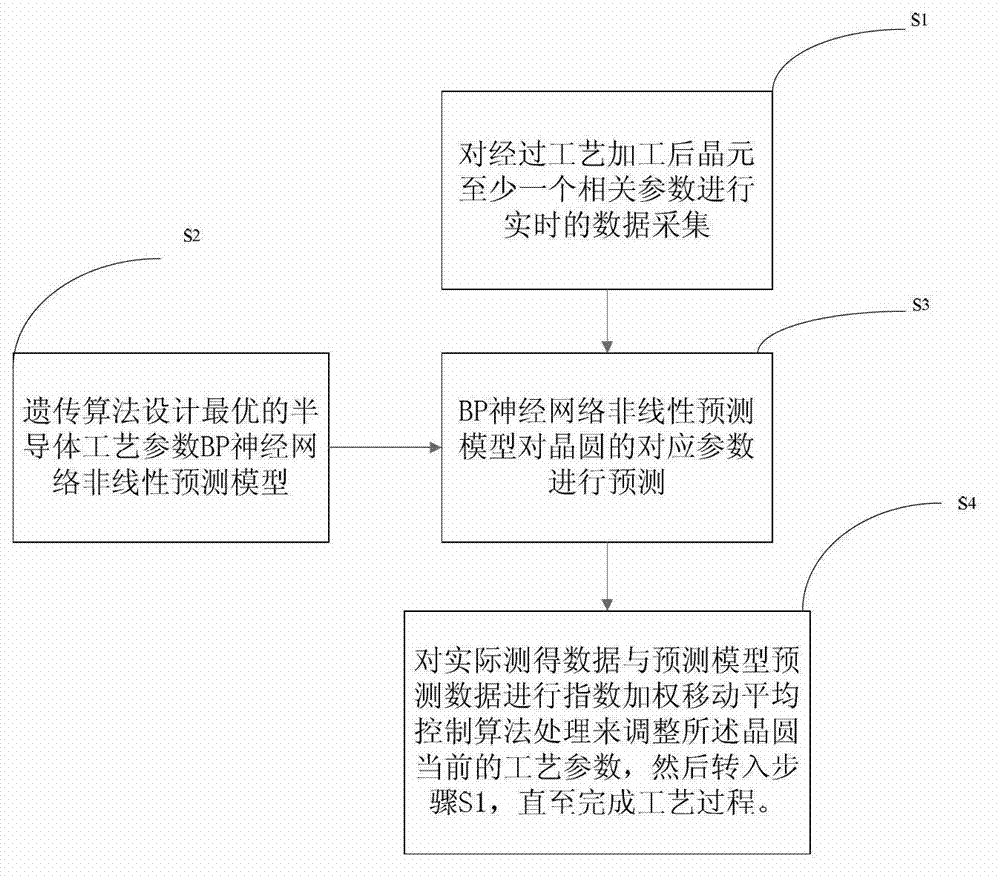
[0038] According to the scheme of the present invention, such as figure 1 As shown, the present invention provides a parameter optimization control method for semiconductor advanced process control, including the following steps: S1, real-time data collection of at least one related process parameter of the wafer after process processing; S2, using genetic algorithm to design the most Optimal semiconductor process parameters BP neural network nonlinear prediction model; S3, using the genetic algorithm to optimize the BP neural network nonlinear prediction model to predict the corresponding process parameters of the wafer; S4: the actual measured data and the prediction model prediction The data is processed by an exponential weighted moving average control algorithm to adjust the current process parameters of the wafer, and then transfer to step S1 until...


PUM


Abstract

The invention discloses a parameter optimization control method of semiconductor advance process control (APC). In semiconductor technological process, a traditional method uses a linear prediction model for the optimization control method of batch process. The parameter optimization control method of the semiconductor advance process control uses an optimized back propagation (BP) neural network prediction model based on genetic algorithm, optimizes the initial weight values and threshold values of the neural network through the genetic algorithm, uses selecting operation, probability crossover and mutation operation and the like according to the fitness function F corresponding to each chromosome, and outputs the optimum solution finally to determine the optimum initial weight value and the threshold value of the BP neural network. The performance of the BP neural network is improved with an additional momentum method and variable learning rate learning algorithm being used, so that the BP neural network after being trained can predict the non-linear model well. The genetic algorithm in the method has good global searching ability, a global optimal solution or a second-best solution with good performance is easy to obtain, and the genetic algorithm well promotes the improvement of modeling ability of the neural network.

Description

technical field [0001] The invention relates to semiconductor process control, in particular to a parameter optimization control method for semiconductor advanced process control, which is used for dynamic setting of process parameters of semiconductor devices between batches and optimal adjustment of control systems. Background technique [0002] With the continuous enhancement of the function and performance of integrated circuit chips and the continuous reduction of the feature size of semiconductor devices, the investment cost of integrated circuit production lines has become very high, so the precise control of semiconductor processes is particularly important, especially for different batches of semiconductors. Run-to-Run (R2R) control of the device. During the production process of semiconductor chips, several different processes are required, such as photolithography, CVD, PVD, etching, etc. Semiconductor advanced process control (APC) can improve the utilization ra...

Claims


Application Information

Patent Timeline
Patent Type & Authority Applications(China)
IPC IPC(8): G05B13/04
Inventor 王巍安友伟杨铿冯世娟王振徐华
Owner 苏科斯(江苏)半导体设备科技有限公司
Why Eureka
Try Eureka