

Forming method for semiconductor device
A semiconductor and device technology, applied in the field of semiconductor device formation, can solve problems such as poor performance, achieve good performance, good quality, and reduce the K value
- Summary
- Abstract
- Description
- Claims
- Application Information
AI Technical Summary
Problems solved by technology
Method used
Image

Examples
Embodiment Construction
[0038] As mentioned in the background art, semiconductor devices formed in the prior art have poor performance in semiconductor integrated circuits.
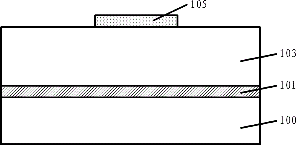
[0039] After doing your research, go ahead and refer to Figure 5 The inventors found that the reason for the poor performance of the semiconductor integrated circuit in the prior art is that there are more interlayer dielectric layers 103 between two adjacent trenches, resulting in a higher effective K value in the interconnection layer.
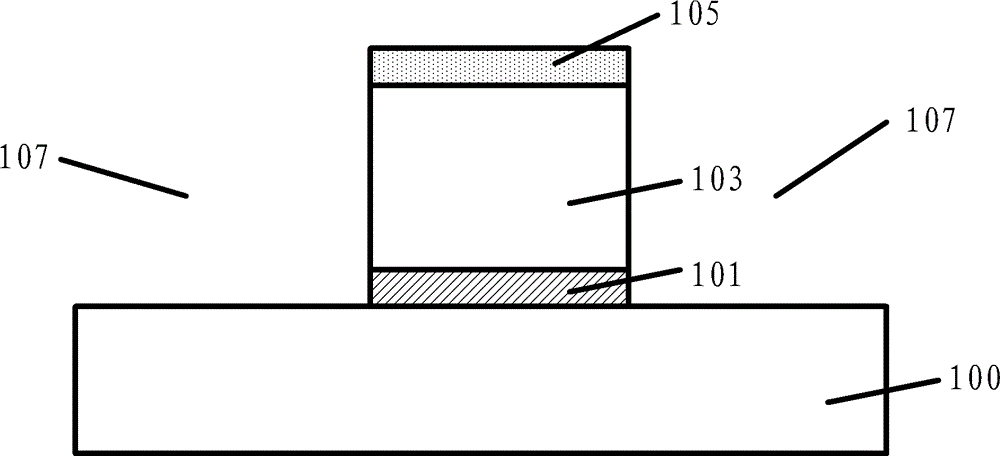
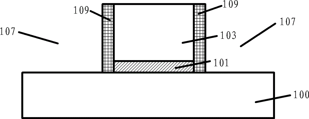
[0040] After further research, the inventors found that if a sacrificial layer is formed by oxidizing the sidewall of the trench 107 without using a deposition process, the process steps can be reduced. Please refer to figure 2 , removing the patterned photoresist layer 105 by using an ashing process (please refer to figure 2 ) while oxidizing the interlayer dielectric layer 103 on the sidewall of the trench 107 to form a sacrificial layer, and then filling the trench 107 with conductive m...
PUM
 Abstract
Description
Claims
Application Information