
a method of exposure

An exposure method and light source technology, applied in the field of exposure, can solve the problems of etching failure, scrapped semiconductor devices, difficult to overcome the diffraction phenomenon of lithography, etc., and achieve the effect of preventing the diffraction phenomenon

Active Publication Date: 2015-12-16
SEMICON MFG INT (SHANGHAI) CORP
View PDF5 Cites 0 Cited by
  • Summary
  • Abstract
  • Description
  • Claims
  • Application Information

AI Technical Summary

Problems solved by technology

[0005] Therefore, in order to improve the quality of lithography in the lithography process, various methods have been adopted, such as immersion lithography, mask using double-layer graphics, off-axis illumination of lithography machines, and phase shifting. Graphical methods, etc., but these methods are difficult to overcome the diffraction phenomenon in the photolithography process
The diffraction phenomenon in the photolithography process will cause the final semiconductor device to fail due to the unclear pattern on the photoresist layer during etching, and the semiconductor device produced will be scrapped.

Method used


Image

  • a method of exposure
  • a method of exposure
  • a method of exposure

Examples


Embodiment Construction

[0025] In order to make the object, technical solution and advantages of the present invention clearer, the present invention will be further described in detail below with reference to the accompanying drawings and examples.

[0026] In the background technology, during the exposure process of photolithography, the reason for the diffraction phenomenon is that the pattern of the mask plate takes away the exposure energy, and makes the exposed light source diverge, and when it is transferred to the photoresist layer of the silicon wafer, the silicon The unexposed areas of the photoresist layer of the wafer are exposed. This situation becomes more pronounced as the feature size of semiconductor devices decreases, such as 200nm contact holes, and the transfer pattern on the silicon wafer caused by diffraction can make small contact holes and small lines difficult to be photolithographic.

[0027] In order to overcome this problem, the present invention forms an excitation area o...


PUM


Abstract

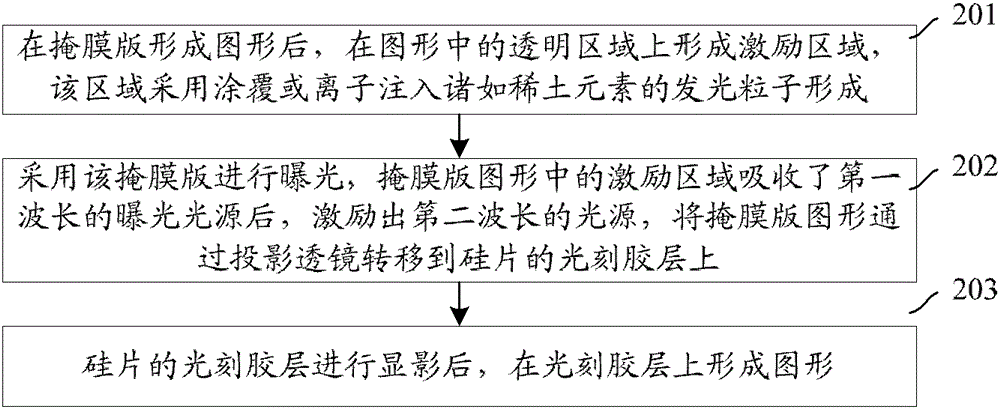
The invention discloses an exposure method and a mask plate for exposure. The method comprises the following steps of: after a graph is formed on the mask plate, forming an excitation area in the transparent area of the graph; when the mask plate is adopted for exposure, after the excitation area formed in the graph of the mask plate absorbs an exposure light source with first wavelength, exciting a light source with second wavelength, and transferring the graph of the mask plate onto a photoresist layer of a silicon wafer via a projection lens; and after the photoresist layer of the silicon wafer is developed, forming a graph on the photoresist layer. Because of the method, exposure energy cannot be taken away by the mask plate, light cannot be diffused, and diffraction during the exposure process can be prevented under the condition that the feature size of a semiconductor is reduced.

Description

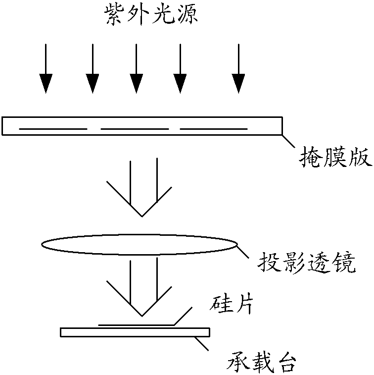
technical field [0001] The invention relates to the technical field of semiconductor manufacturing, in particular to an exposure method. Background technique [0002] In the semiconductor manufacturing process, photolithography is involved. Photolithography technology is to use the optical system to accurately project and expose the pattern on the mask onto the silicon wafer coated with the photoresist layer, and then the photoresist layer on the silicon wafer is developed to obtain the pattern. [0003] figure 1 It is a schematic diagram of the structure of the photoresist layer that transfers the pattern on the mask plate to the silicon wafer in the prior art. This structure is the structure of the photolithography machine. As shown in the figure, the mask plate has a transparent area and an opaque area. These areas form the pattern that is transferred to the surface of the photoresist layer of the silicon wafer. Place the silicon wafer coated with a photoresist layer o...

Claims


Application Information

Patent Timeline
Patent Type & Authority Patents(China)
IPC IPC(8): G03F7/20G03F1/54
Inventor 王辉王伟斌
Owner SEMICON MFG INT (SHANGHAI) CORP
Learn More