
Method of achieving fast driving of area array charge coupled device (CCD) by means of inductive charge accumulation

A technology of inductive charge and area array, applied in the field of photoelectric imaging, can solve the problems that area array CCD cannot be realized, and achieve the effect of expanding the light adaptation range, convenient realization and reasonable design.

Active Publication Date: 2013-05-15
EAST CHINA INST OF OPTOELECTRONICS INTEGRATEDDEVICE
View PDF3 Cites 9 Cited by
  • Summary
  • Abstract
  • Description
  • Claims
  • Application Information

AI Technical Summary

Problems solved by technology

[0006] Purpose of the present invention: In order to solve the problem that the area array CCD in the prior art cannot be realized or needs to apply the shutter technology to realize high-speed dynamic image imaging, provide a method for quickly driving the area array CCD by using induced charge accumulation

Method used


Image

  • Method of achieving fast driving of area array charge coupled device (CCD) by means of inductive charge accumulation
  • Method of achieving fast driving of area array charge coupled device (CCD) by means of inductive charge accumulation
  • Method of achieving fast driving of area array charge coupled device (CCD) by means of inductive charge accumulation

Examples


Embodiment Construction

[0035] The present invention will be further described below in conjunction with the accompanying drawings and specific applications.

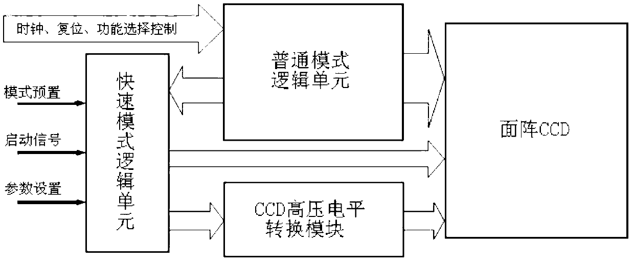
[0036] figure 1 It is a functional block diagram, and various specific implementation schemes can follow this diagram.

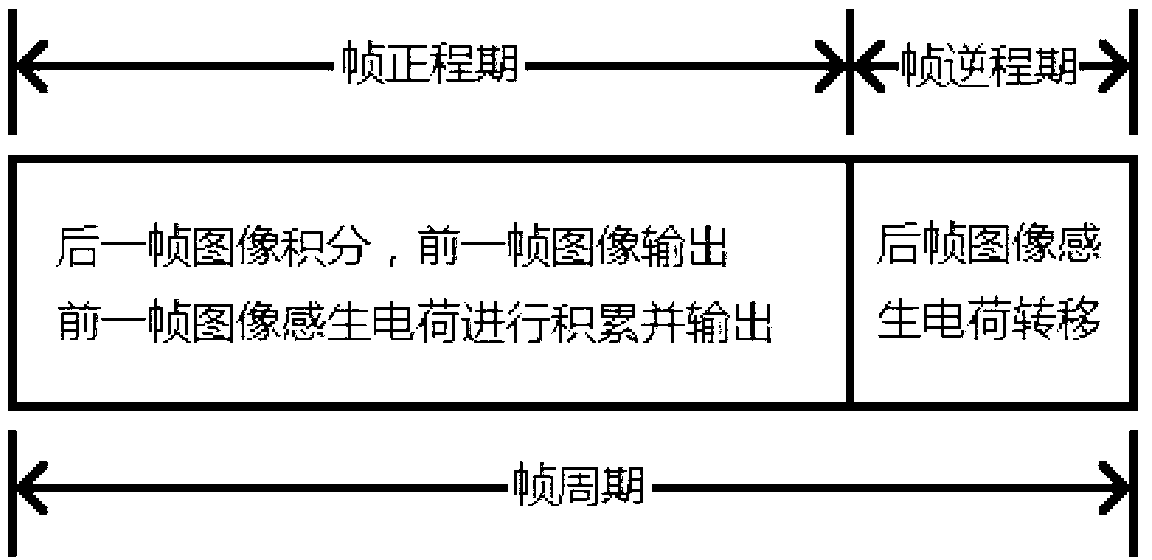
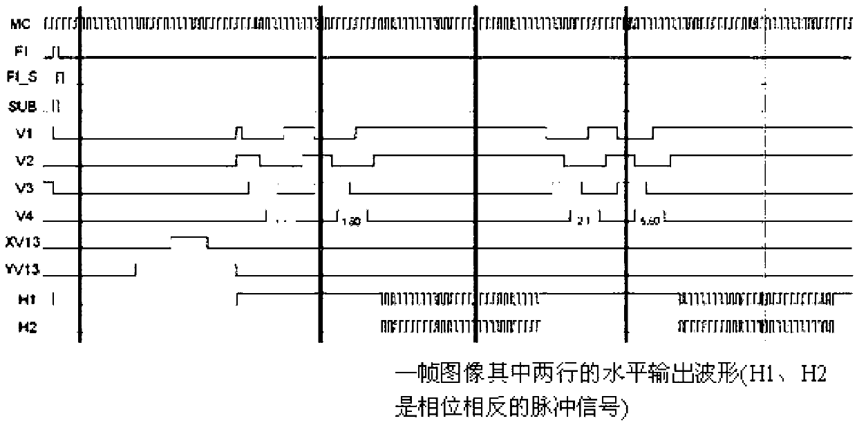
[0037] figure 2 It is a timing diagram for fast driving of a frame image by an area array CCD using induced charge accumulation. The complete frame period of an area array CCD image can be divided into a frame forward period and a frame reverse period; in the frame forward period, the area array CCD photosensitive unit Image integration is carried out, and at the same time, the induced charges of the previous frame image temporarily stored in the storage area begin to transfer to the horizontal shift register, and the induced charge accumulation occurs and row output begins, and the entire output of the induced charges of the previous frame image is completed during the frame normal period . The frame forward period ends...


PUM


Abstract

The invention discloses a method of achieving fast driving of an area array charge coupled device (CCD) by means of inductive charge accumulation. The method comprises the steps that model parameter setting is carried out according to imaging requirements; an area array CCD driving schedule is generated; the area array CCD enters into an integration phase and inductive charges are generated; the integration phase ends and the inductive charges are transferred to a storage area; the area array CCD enters into the next integration phase; the inductive charges are transferred to a horizontal shifting register; the inductive charge accumulation is carried out by repeating the previous operation according to a given parameter; the horizontal shifting register outputs a line of inductive charges; the previous operation is repeated according to the given parameter until inductive charges of one frame of images are all output; and output of the next frame of images is carried out by repeating the fourth step to the ninth step. According to the method of achieving the fast driving of the area array CCD by means of the inductive charge accumulation, fast output of inductive charges of the area array CCD is achieved by means of the model parameter setting under the circumstance that external imaging environment changes, and the light adaptation range of the area array CCD can be widened greatly.

Description

technical field [0001] The invention relates to a method for quickly driving an area array CCD by using induced charge accumulation, and belongs to the technical field of photoelectric imaging. Background technique [0002] The pixels of an area array CCD device are arranged as a plane, which is a combination of several rows and columns. Generally speaking, there are three most common structural forms for an area array CCD image sensor: (1) Inter-row transfer: also known as It is an alternate column transfer type, and the structure adopts the alternate arrangement of the photosensitive area and the light-shielding transfer area. When the photocharge is read out, the mask storage area between the two columns is used to store the photocharge packet, and the newly generated photocharge packet starts to accumulate in the column without the mask, and the storage unit in the shading area corresponds to the photosensitive unit one by one. When the exposure time is over, the inform...

Claims


Application Information

Patent Timeline
Patent Type & Authority Applications(China)
IPC IPC(8): H04N5/353H04N5/372H04N5/357
Inventor 刘庆飞邹继鑫张猛蛟戴放
Owner EAST CHINA INST OF OPTOELECTRONICS INTEGRATEDDEVICE
Learn More