Electronic equipment and imaging method thereof

An electronic device and image technology, which is applied in TV, color TV, image communication, etc., can solve the problem of not being able to obtain clear images of objects, and achieve the effect of improving image collection distance and good image effect

Active Publication Date: 2013-06-05
LENOVO (BEIJING) LTD
View PDF10 Cites 4 Cited by
  • Summary
  • Abstract
  • Description
  • Claims
  • Application Information

AI Technical Summary

Problems solved by technology

However, the bidirectional OLED display device in the prior art uses CMOS light sensing, so it can only sense light at a small distance, and can only collect images of items that are closer to its display screen.
When the item is far away from the display screen, a clear image of the item cannot be obtained

Method used


Image

  • Electronic equipment and imaging method thereof
  • Electronic equipment and imaging method thereof

Examples


Embodiment 1

[0063] An embodiment of the present invention provides an electronic device for displaying an image of an item while collecting the image. The electronic device includes at least one display unit and at least one image acquisition unit; wherein, the display unit is arranged adjacent to the image acquisition unit, and a lens for collecting optical signals is arranged in the image acquisition unit.

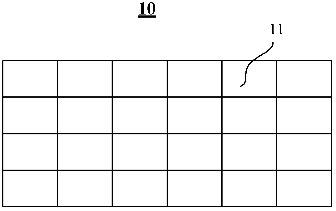
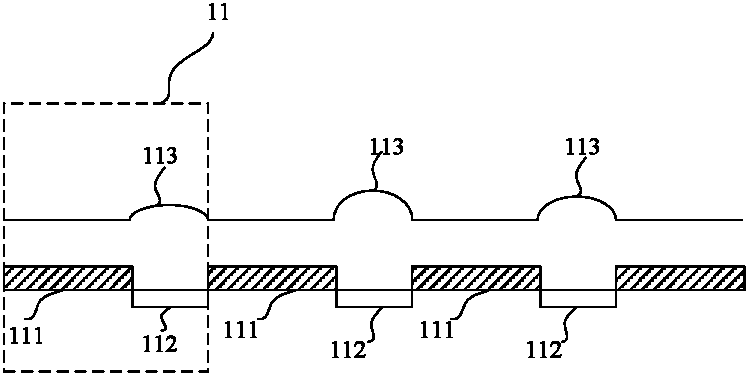
[0064] In the above structure of this embodiment, the electronic device may specifically be a CMOS-OLDE display device. Please refer to figure 1 , shows a schematic top view of the electronic device 10, the electronic device includes a display panel on which a plurality of sub-pixel units 11 are formed. Please refer to figure 2, each sub-pixel unit 11 includes a display unit 111 and an image acquisition unit, wherein the image acquisition unit specifically includes a photodiode unit 112 for converting optical signals into electrical signals and is arranged at The lens 113 on the...

Embodiment 2

[0079] The embodiment of the present invention also provides another electronic device, the electronic device includes a first component and a second component, wherein, the first component can be arranged on the first surface of the electronic device, and the second component can be arranged on the electronic device second surface.

[0080] Specifically, the first component includes at least one first image acquisition unit, and the first image acquisition unit is provided with a first lens for collecting optical signals. Wherein the first image acquisition unit may also include a first photodiode unit for converting optical signals into electrical signals, and the first lens is arranged within the range of the photosensitive viewing angle of the first photodiode unit, so that the incident light reach the first photosensitive diode unit through the first lens.

[0081] Here, the first lens may be an optical microlens, wherein the at least one first image acquisition unit has...


PUM


Abstract

The invention provides electronic equipment and an imaging method thereof, wherein the electronic equipment comprises at least one display unit and at least one image acquisition unit, the display unit and the image acquisition unit are adjacently distributed, and each image acquisition unit is provided with an optical lens used for collecting optical signals. The electronic equipment and the imaging method of the electronic equipment can achieve a good imaging effect.

Description

technical field [0001] The invention relates to the technical field of imaging and display, in particular to an electronic device and an imaging method thereof. Background technique [0002] Human-computer interaction has become the trend of digital life development in the future. People hope to have such a display device, which can display the image of the item while collecting the image of the item. [0003] With the rapid development of organic light emitting diode (OLED) technology, a bidirectional OLED display device has emerged, which includes a display screen. The device is capable of collecting images of items above the display screen and displaying them on the display screen. However, the bidirectional OLED display device in the prior art is sensitive to light through CMOS, so it can only sense light at a small distance, and can only collect images of items that are relatively close to its display screen. When the item is far away from the display screen, a clear...

Claims


Application Information

Patent Timeline
Patent Type & Authority Applications(China)
IPC IPC(8): G09F9/33H04N5/374
CPCG09F9/33H04N5/374G09G5/00H04N5/335H04N5/23293G09G2360/144G06F3/0412G06F3/042H04N23/67H04N25/00H04N25/76
Inventor 牛泉阳光杨锦平尚可
Owner LENOVO (BEIJING) LTD
Why Eureka
Try Eureka