Method and device for simultaneously accessing multiple solid-state disks
A technology of storage location and physical address, applied in the direction of memory address/allocation/relocation, input/output to the record carrier, etc., to achieve the effect of prolonging the service life
- Summary
- Abstract
- Description
- Claims
- Application Information
AI Technical Summary
Problems solved by technology
Method used
Image
Examples
Embodiment Construction
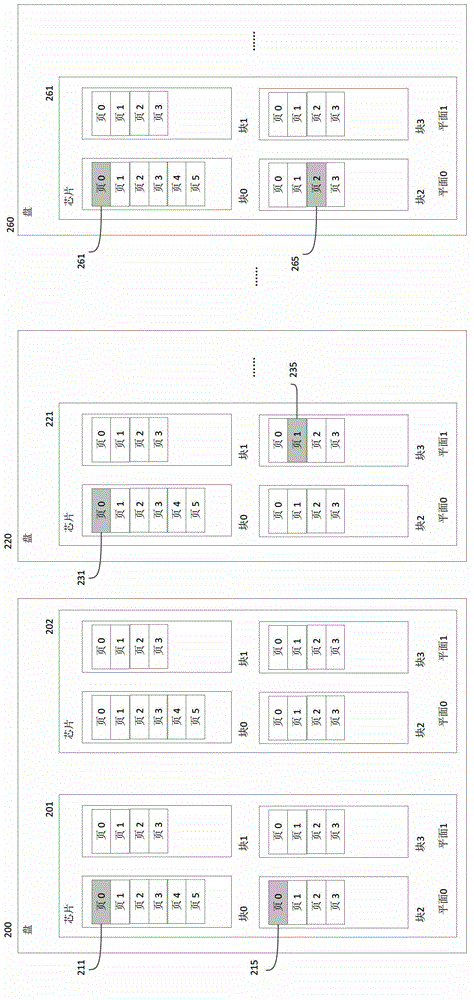
[0073] figure 2 is the data organization of the storage device according to the embodiment of the present invention. The storage device includes a solid state disk 200 , a solid state disk 220 . . . a solid state disk 260 . Each SSD can be a standard size 3.5, 2.5 or 1.8 inch drive. The solid state disk 200 may include a flash memory chip 201 and a flash memory chip 202 . The solid state disk 220 includes a flash memory chip 221 , and the solid state disk 260 includes a flash memory chip 261 . The solid state disk 200 may also include different numbers of flash memory chips. And the solid state disk 200 , the solid state disk 220 and the solid state disk 260 may respectively include different numbers and / or different capacities of flash memory chips. The flash chips in an SSD can be organized into multiple channels to trade off between the number of interface pins used and the parallel access of multiple flash chips. For example, Chinese patent applications with applicat...
PUM
 Abstract
Description
Claims
Application Information


