Supercharge Your Innovation With Domain-Expert AI Agents!

Optical coupling module and manufacturing method thereof

An optical coupling and optical module technology, which is applied in the coupling of optical waveguides and other directions, can solve problems such as affecting the coupling effect and the position of the optical module is prone to deviation, and achieves the effect of increasing the light-receiving range.

Inactive Publication Date: 2013-06-19
HONG FU JIN PRECISION IND (SHENZHEN) CO LTD +1
View PDF4 Cites 10 Cited by
  • Summary
  • Abstract
  • Description
  • Claims
  • Application Information

AI Technical Summary

Problems solved by technology

However, during the die bonding process, the position of the optical module is prone to deviation, which affects the light coupling effect

Method used


Image

  • Optical coupling module and manufacturing method thereof
  • Optical coupling module and manufacturing method thereof
  • Optical coupling module and manufacturing method thereof

Examples


Embodiment Construction

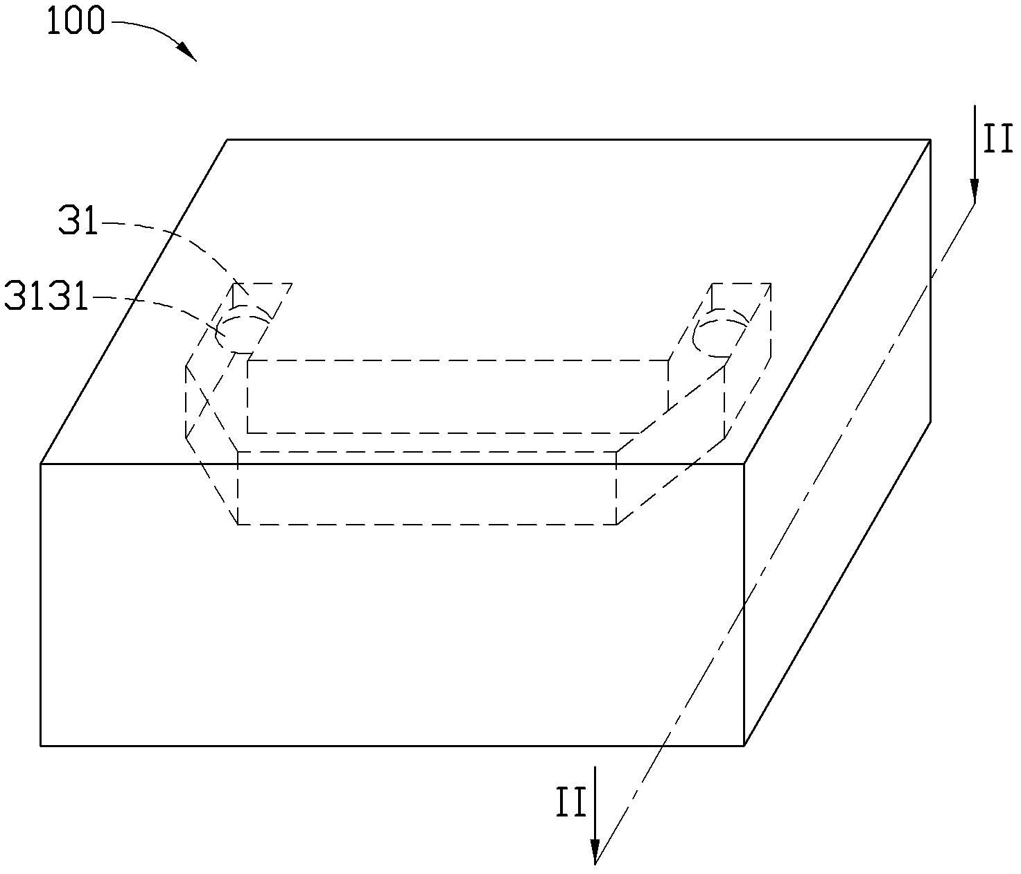
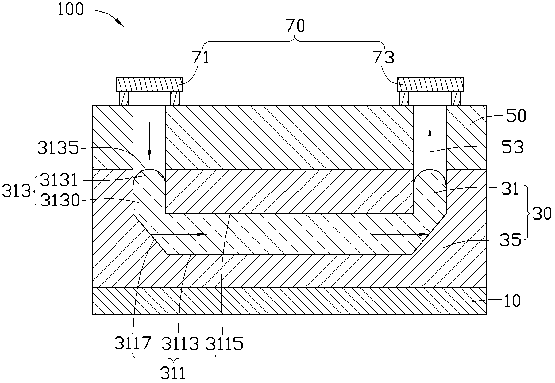
[0019] see figure 1 and figure 2 Yes, the optical coupling module 100 of this embodiment includes a substrate 10 , an optical waveguide 30 , a circuit substrate 50 and an optical module 70 . The optical waveguide 30 is located between the substrate 10 and the circuit substrate 50 , and the optical module 70 is installed on the circuit substrate 50 .

[0020] The substrate 10 may be formed of an insulating material such as resin, glass, or ceramics. The substrate 10 may also be formed of a conductive material such as metal. In this case, an insulating film needs to be formed on the mounting surface on which the integrated circuit chip is mounted. Preferably, the substrate 10 has high thermal conductivity. Circuits can also be laid on the substrate 10 for driving and controlling the operation of the optical module 70 or other components.

[0021] The optical waveguide 30 is formed on the substrate 10 for transmitting optical signals. The optical waveguide 30 includes a cor...


PUM


Abstract

An optical coupling module comprises a substrate, optical waveguide, a circuit substrate and an optical module. The optical waveguide is arranged between the substrate and the circuit substrate. The optical waveguide comprises a core layer and a wrapping layer. The core layer is provided with an optical coupling surface. Light holes corresponding to the optical coupling surface and arranged through the circuit substrate are formed in the circuit substrate. The optical module is arranged on the light holes to penetrate and is used for optical coupling with the optical coupling surface through the light holes. The optical coupling surface is almost convex-lens-shaped and capable of gathering light signals projected into the core layer to transmit, and gathering light signals emitted from the core layer to transmit. According to the optical coupling module, a certain offset happens during the process of wafer sticking, and the optical coupling effect is not influenced. The invention further provides a manufacturing method of the optical coupling module.

Description

technical field [0001] The invention relates to an optical coupling module and a preparation method thereof, in particular to an optical coupling module capable of improving the optical coupling effect and a preparation method thereof. Background technique [0002] In recent years, optical communication has a development trend of high speed and large capacity. Generally speaking, in optical communication, it is necessary to use optical components to convert photoelectric signals, and to use optical waveguides to transmit optical signals. [0003] In the existing optical coupling module, the optical waveguide is formed between the substrate and the circuit substrate. The optical waveguide consists of a core layer (Core) and a cladding layer (Clad). The core layer has a planar light coupling surface. The cladding covers the core layer and exposes the light coupling surface. A light-transmitting hole is formed on the circuit substrate corresponding to the light-coupling sur...

Claims


Application Information

Patent Timeline
Patent Type & Authority Applications(China)
IPC IPC(8): G02B6/42G02B6/255G02B6/24
Inventor 李秉衡
Owner HONG FU JIN PRECISION IND (SHENZHEN) CO LTD
Features
  • R&D
  • Intellectual Property
  • Life Sciences
  • Materials
  • Tech Scout
  • Unparalleled Data Quality
  • Higher Quality Content
  • 60% Fewer Hallucinations
Learn More