A MOS device with broadband characteristics based on teo2/pentacene composite

A technology of MOS devices and composite materials, applied in semiconductor/solid-state device manufacturing, semiconductor devices, electric solid-state devices, etc., can solve the problems of reduced other device parameters, poor amplitude-frequency characteristics, high cost, etc. Reduced, the effect of excellent characteristics

Inactive Publication Date: 2015-08-26
CHONGQING UNIV
View PDF4 Cites 0 Cited by
  • Summary
  • Abstract
  • Description
  • Claims
  • Application Information

AI Technical Summary

Problems solved by technology

Generally, the process involved in this type of MOS device is relatively complicated, especially the cost of the doping step is relatively high
In addition, the physical size of such devices can only be limited within a certain range
More importantly, such devices have great limitations in the operation of high-frequency circuits, and their amplitude-frequency characteristics are poor
At present, in order to solve the defects of devices working on high-frequency circuits, most of the methods are to use heavy doping process or change the types of impurities, but this method will also cause the reduction of other parameters of the device, and the preparation process is relatively complicated, and there are still some problems. inadequacies of

Method used


Image

  • A MOS device with broadband characteristics based on teo2/pentacene composite
  • A MOS device with broadband characteristics based on teo2/pentacene composite
  • A MOS device with broadband characteristics based on teo2/pentacene composite

Examples


Embodiment Construction

[0022] The present invention will be further described below in conjunction with the accompanying drawings and specific embodiments.

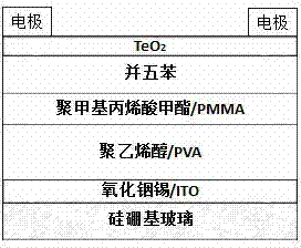
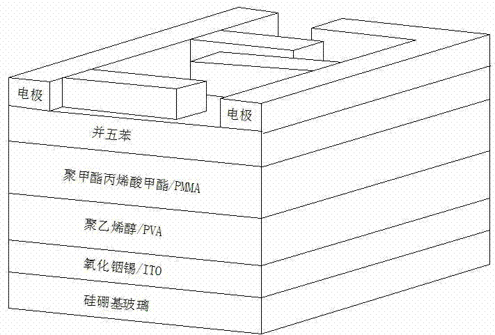
[0023] like figure 1 and figure 2 As shown, a TeO-based 2 / Pentacene composite material MOS device with broadband characteristics, the structure of the MOS device is an "inverted" structure, that is, the entire MOS device is prepared on the gate of the device, unlike the traditional silicon material as the substrate MOS devices are completely different. Indium tin oxide sputtered on silicon-boron-based substrate glass is used as the gate of the device. Using the solution prepared by polyvinyl alcohol PVA and polymethyl methacrylate PMMA as raw materials, two layers of materials are grown on the gate in turn by the method of uniform coating, and the composite of the two forms an insulating layer, in which the polyvinyl alcohol layer make contact with the grid. On this basis make based on TeO 2 / Pentacene composite material active active ...


PUM


Abstract

The invention discloses a metal oxide semiconductor (MOS) apparatus based on a TeO2 / pentacene composite material and having a broadband characteristic. The apparatus comprises a source, a grid and a drain, wherein from bottom to top, the MOS apparatus has the following structure: glass is taken as a substrate and indium tin oxide (ITO) is taken as the grid, a dual-layer material structure of polyvinyl alcohol (PVA) and polymethyl methacrylate (PMMA) is used as an insulating layer, and a TeO2 / pentacene composite material is taken as an active layer; both the source and the drain adopt gold as electrodes, and the source and the drain are in interdigital structures. The apparatus disclosed by the invention is an active MOS apparatus which controls conductivity of solid material through an electric field. The apparatus represents a remarkable broadband characteristic, and frequency band is comparatively wide even on an amplitude-frequency characteristic; so that the apparatus disclosed by the invention has a good application prospect in sensors, high-frequency electronic circuits, large-scale integration circuits and active display fields.

Description

technical field [0001] The invention relates to a semiconductor device, in particular to a MOS device with broadband characteristics. Background technique [0002] In the prior art, a MOS device includes a source, a gate, and a drain. The main structure of a traditional MOS device is to use a silicon wafer as a substrate, and oxidize the middle part of the silicon wafer to produce SiO 2 The oxide layer is used as an insulating layer, and then a metal electrode is grown on the insulating layer by thermal evaporation as a gate electrode. The source and drain electrodes are also longer than the original silicon that has not been oxidized by thermal evaporation. Generally, the process involved in this type of MOS device is relatively complicated, especially the cost of the doping step is relatively high. In addition, the physical size of such devices can only be limited within a certain range. More importantly, such devices have great limitations in the operation of high-freq...

Claims


Application Information

Patent Timeline
Patent Type & Authority Patents(China)
IPC IPC(8): H01L51/05H01L51/30H01L51/40
Inventor 甘平李奋展童中华吴立强陈卓刘德鹏刘涛刘冬翠
Owner CHONGQING UNIV
Why Eureka
Try Eureka