Method for preparing scanning electron microscope (SEM) sample or transmission electron microscope (TEM) sample protection layer by using focused ion beam (FIB) technology

A technology of protective layer and metal protective layer, which is applied in the field of preparing SEM or TEM sample protective layer by using FIB technology, can solve the problems such as the interface is not clear enough, and achieve the effect of improving the interface clarity, improving the quality of analysis, and being simple and convenient to use

Active Publication Date: 2013-07-10
SHANGHAI HUALI MICROELECTRONICS CORP
View PDF5 Cites 23 Cited by
  • Summary
  • Abstract
  • Description
  • Claims
  • Application Information

AI Technical Summary

Problems solved by technology

[0005] The purpose of the present invention is to provide a method for preparing a SEM or TEM sample protective layer using FIB technology to solve the problem that the interface of the sample surface and the protective layer on the sample surface is not clear enough when imaging due to the relatively close materials

Method used


Image

  • Method for preparing scanning electron microscope (SEM) sample or transmission electron microscope (TEM) sample protection layer by using focused ion beam (FIB) technology
  • Method for preparing scanning electron microscope (SEM) sample or transmission electron microscope (TEM) sample protection layer by using focused ion beam (FIB) technology
  • Method for preparing scanning electron microscope (SEM) sample or transmission electron microscope (TEM) sample protection layer by using focused ion beam (FIB) technology

Examples


Embodiment Construction

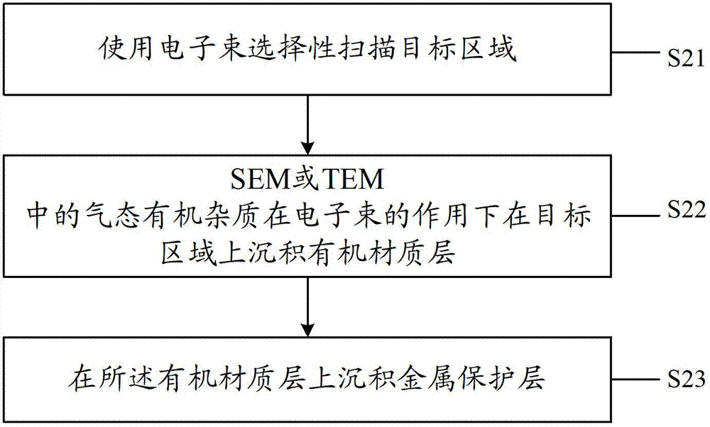
[0016] The method for preparing the SEM or TEM sample protective layer using the FIB technology proposed by the present invention will be further described in detail below in conjunction with the accompanying drawings and specific examples. Advantages and features of the present invention will be apparent from the following description and claims. It should be noted that all the drawings are in a very simplified form and use imprecise scales, and are only used to facilitate and clearly assist the purpose of illustrating the embodiments of the present invention.
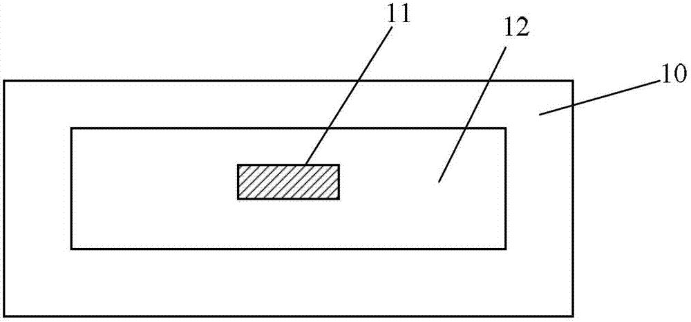
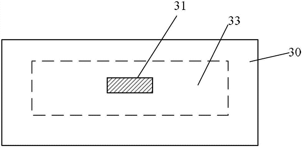
[0017] The core idea of ​​the present invention is that, in the method for preparing the protective layer of SEM or TEM samples provided by the present invention using FIB technology, before using the FIB technology for conventional sample preparation, the electron beam is used to deposit an organic material layer on the target area, so that the target area For samples with a metal surface, due to the strong contrast ...


PUM


Abstract

The invention provides a method for preparing a scanning electron microscope (SEM) sample or a transmission electron microscope (TEM) sample protection layer by using a focused ion beam (FIB) technology, and is applied to samples of which target surfaces are made of metal. The method comprises the following steps of: selectively scanning a target region by an electronic beam; under the action of the electronic beam, depositing an organic material layer on the target region by gaseous organic impurities in an SEM or a TEM; and depositing a metal protection layer on the organic material layer. By using the method for preparing the SEM sample or the TEM sample protection layer by using the FIB technology, before the sample is prepared by using the FIB technology, the organic material layer is deposited on the target region by using the electronic beam, so that the surface of the target region serves as the sample made of the metal; a deposited organic material and a metal material on the surface of the target region are greatly contrasted, so that the interface definition of the metal surface of the SEM or TEM sample which is required to be precisely positioned is greatly improved; and the analysis quality of the SEM or TEM is improved.

Description

technical field [0001] The invention relates to the technical field of semiconductor manufacturing, in particular to a method for preparing a SEM or TEM sample protective layer using FIB technology. Background technique [0002] The Focused Ion Beam (FIB for short) system is a microdissection instrument that uses an electric lens to focus the ion beam into a very small size. Transmission electron microscope (TEM for short) projects an accelerated and concentrated electron beam onto a very thin sample, and the electrons collide with atoms in the sample to change their direction, resulting in solid angle scattering. Scanning Electron Microscope (hereinafter referred to as SEM) is a material characterization technology equipment mainly used in the observation and imaging of material surface topography. Although the SEM system or TEM is in a high vacuum state, there are still some gaseous organic impurities that will be deposited in the scanning area in the form of solid under ...

Claims


Application Information

Patent Timeline
Patent Type & Authority Applications(China)
IPC IPC(8): G01N1/28
Inventor 陈强
Owner SHANGHAI HUALI MICROELECTRONICS CORP
Why Eureka
Try Eureka