Device and method for testing field programmable gate array (FPGA) development board

A development board and test unit technology, applied in the field of FPGA testing, can solve problems such as poor contact, dense pin spacing, poor welding, etc.

Inactive Publication Date: 2013-07-24
青岛中星微电子有限公司
View PDF9 Cites 4 Cited by
  • Summary
  • Abstract
  • Description
  • Claims
  • Application Information

AI Technical Summary

Problems solved by technology

[0004] The technical problem to be solved by the present invention is to provide a device and method for testing FPGA development boards, which are used to solve the problems in the prior art that the pins in the FPGA development board are dense and the spacing is small, and poor welding or poor contact are prone to occur.

Method used


Image

  • Device and method for testing field programmable gate array (FPGA) development board
  • Device and method for testing field programmable gate array (FPGA) development board
  • Device and method for testing field programmable gate array (FPGA) development board

Examples


Embodiment Construction

[0019] In order to make the technical problems, technical solutions and advantages to be solved by the present invention clearer, the following will describe in detail with reference to the drawings and specific embodiments.

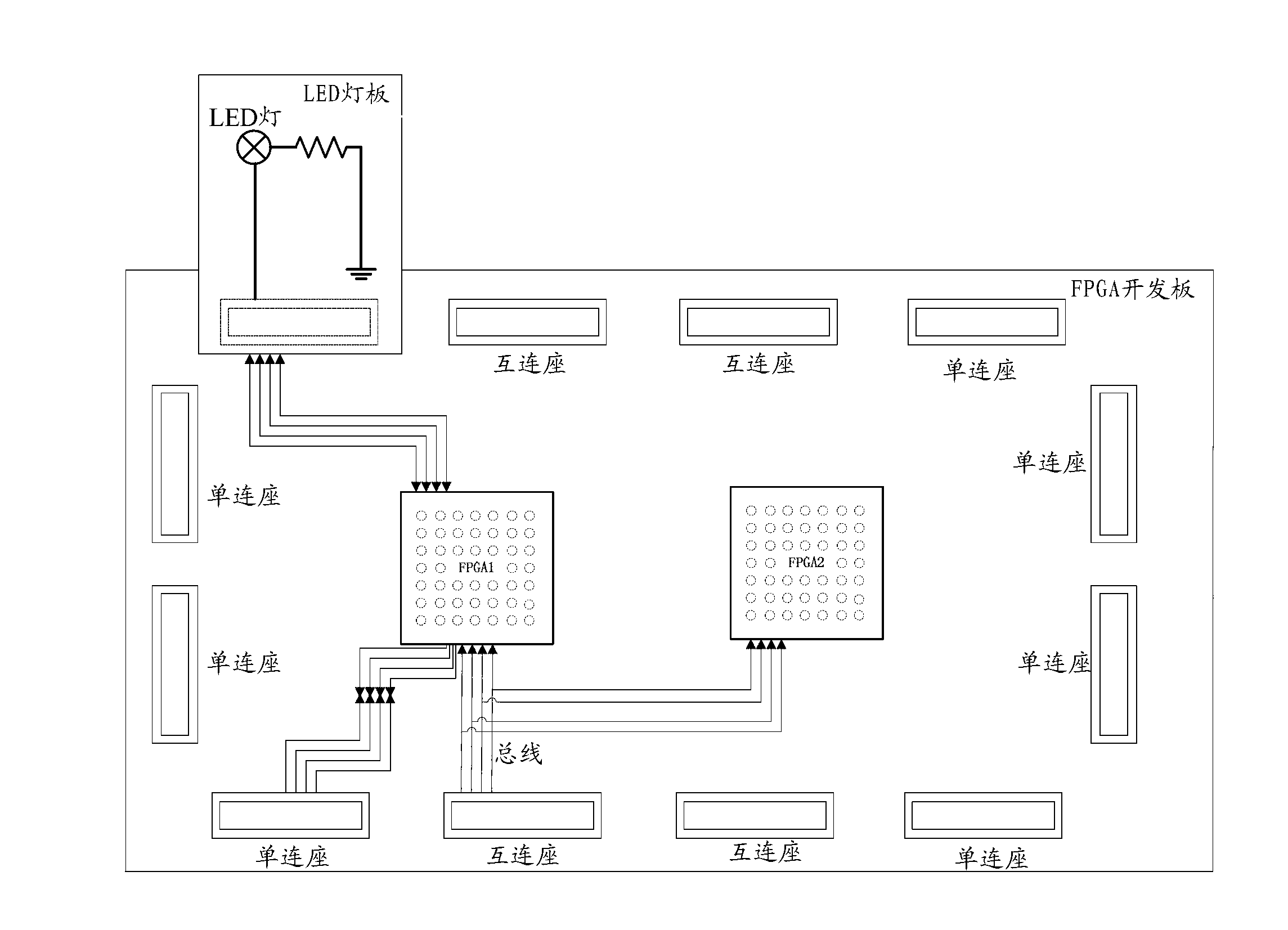
[0020] Embodiments of the present invention provide a device for testing FPGA development boards, such as figure 1 As shown, the FPGA development board includes an FPGA chip,

[0021] Devices include:

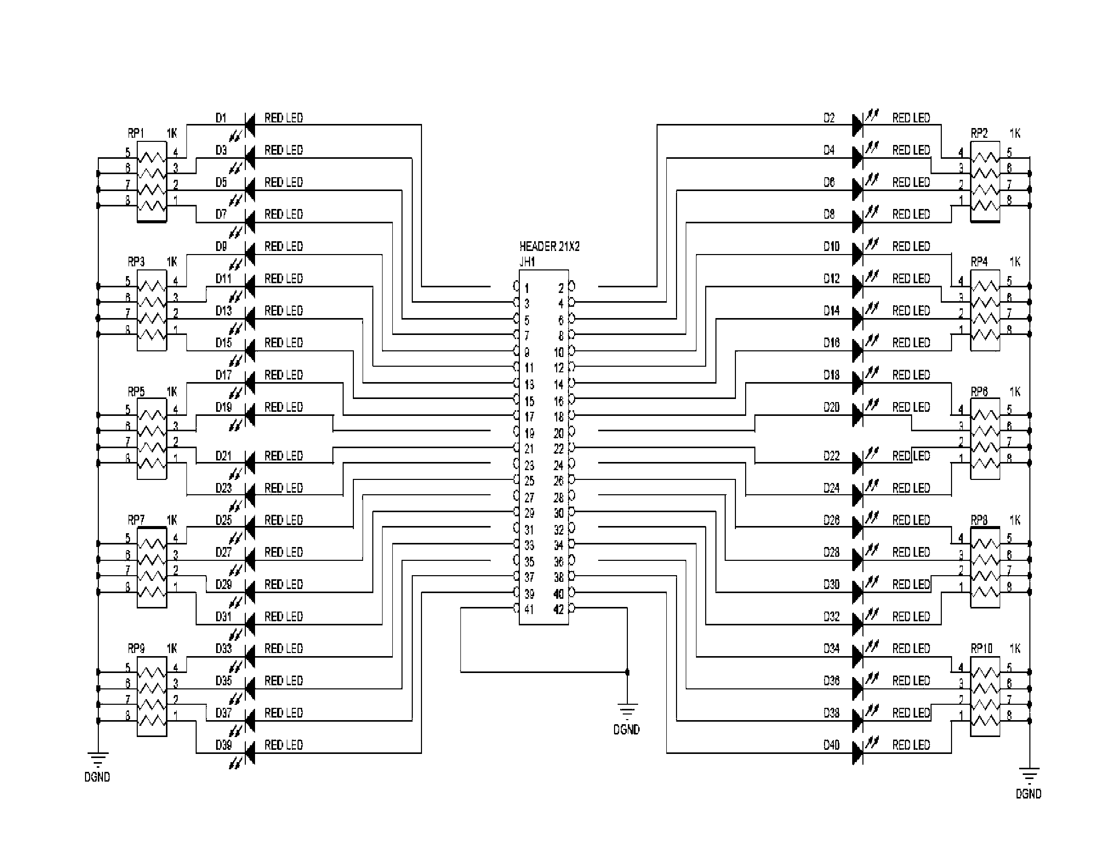
[0022] The LED light board includes a plurality of LED pins, each LED pin is connected to a corresponding LED light, the negative terminals of all LED lights are grounded, and the LED light is lit when the corresponding LED pin is at a high potential;

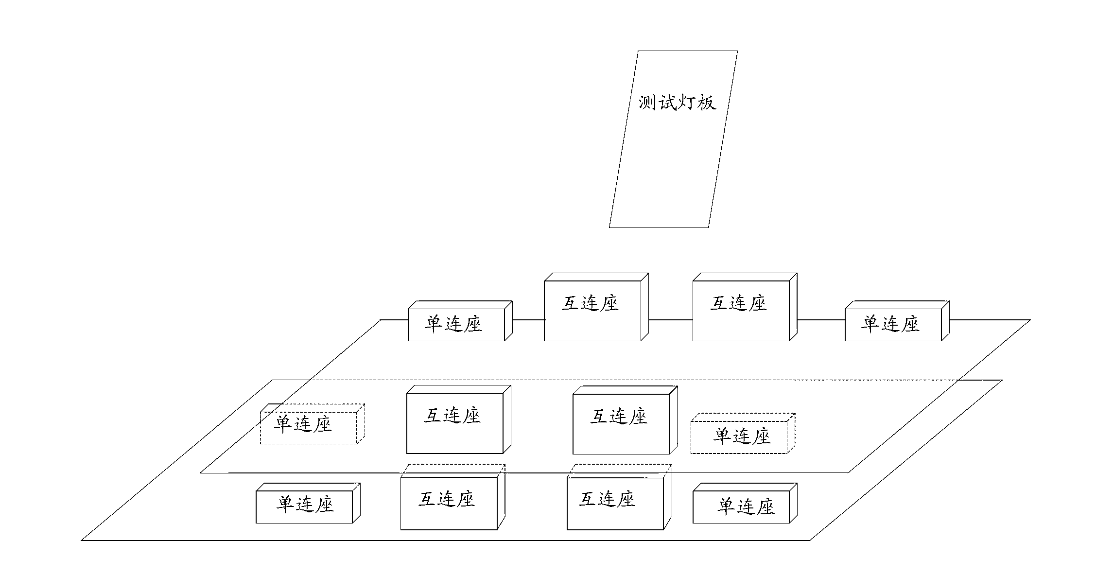
[0023] The arrangement of the LED pins is consistent with the arrangement of the communication pins of the high-speed seat in the FPGA development board, and supports electrical connection with the communication pins;

[0024] The communication pins of the high-speed seat are electrically connected to th...


PUM


Abstract

The invention provides a device and a method for testing a field programmable gate array (FPGA) development board. The device comprises a light-emitting diode lamp plate, LED tube feet and a testing unit. A negative end of each LED lamp is connected with the ground and connected with a corresponding LED tube foot. Each LED lamp is lightened when a corresponding LED tube foot is in high potential. The LED tube feet are used for being electrically connected with communication tube feet of a high-speed seat in the FPGA development board. The communication tube feet of the high-speed seat are correspondingly and electrically connected with function tube feet of an FPGA chip. The testing unit is connected with a JTAG port of the FPGA development board and is used for setting breakover rules of all the function tube feet of the FPGA chip and acquiring breakover conditions of the function tube feet and the communication tube feet according to on-off of the LED lamps corresponding to the function tube feet and the communication tube feet. When the function tube feet are switched between high potential and low potential according to the breakover rules, the LED lamp plate, corresponding to the function tube feet, in the lamp plate can be turned on or turned off, so that detection that whether the function tube foot / the communication tube foot in the position is good in contact or not is completed.

Description

technical field [0001] The present invention relates to the technology of testing FPGA, particularly a kind of device and method of testing FPGA development board. Background technique [0002] Field Programmable Gate Array (FPGA, Field Programmable Gate Array) development board includes two FPGA chips, each FPGA chip usually has 4 single-connected sockets, and two FPGA chips can also communicate through 4 interconnected sockets . [0003] The existing technology has the following problems: the pins in the FPGA development board are dense, the spacing is small, and it is very easy to have poor welding, and the metal shrapnel of the FPGA development board will oxidize after a period of time, and the contact is poor, which affects the function of the entire FPGA development board . Contents of the invention [0004] The technical problem to be solved by the present invention is to provide a device and method for testing FPGA development boards, which are used to solve the ...

Claims


Application Information

Patent Timeline
Patent Type & Authority Applications(China)
IPC IPC(8): G01R31/02
Inventor 林艳芳
Owner 青岛中星微电子有限公司
Why Eureka
Try Eureka