
Patsnap Eureka
For R&D, Patsnap Eureka makes reading and utilizing patents & technical documents easy.
Patsnap Eureka AIR
Designed for self-driven R&D workflows. Generate viable solutions, solve complex R&D challenges, empower your innovation with AI.

Patsnap Eureka Materials
Designed for material experts only. Revolutionize your material R&D, from search, analyze, to developing new materials.

TechResearch
Generate reliable direction feasibility study reports for your R&D in just a few steps.

TechSeek
Discover and master advanced knowledge NOW. Basics, ideas, possibilities, all at once.

TechMind
As an expert in R&D Theories, TechMind can generates customized viable solutions instantly.

TechRisk
Analyze your overall solution with one click, know your potential R&D risks in advance.

TechMonitor
Get weekly tech updates, stay abreast of the latest tech innovations and key insights.
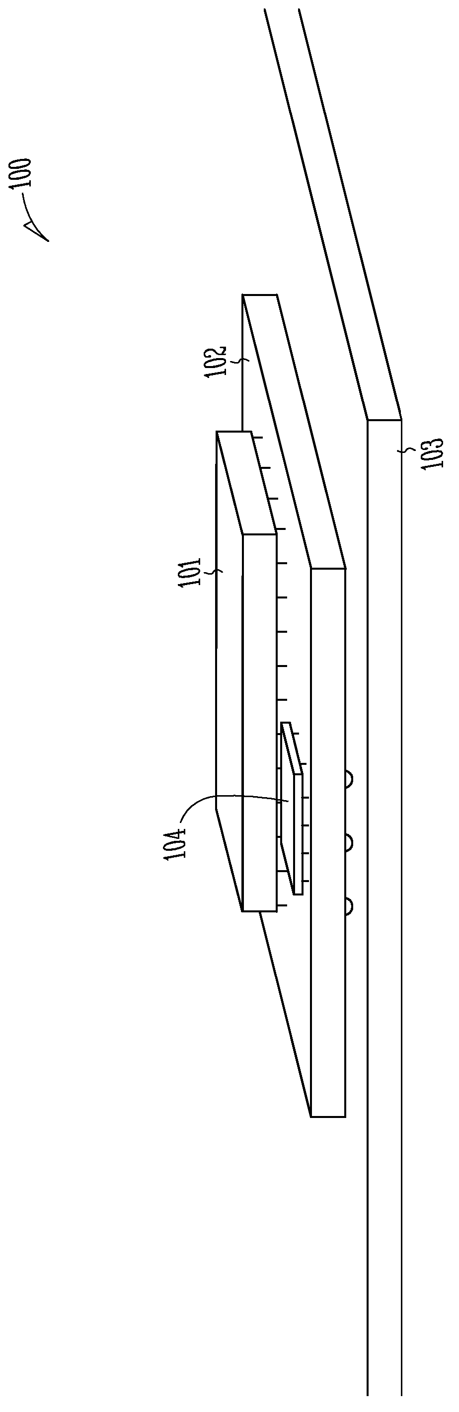
Multi-die MEMS package
A controller and device layer technology, applied in the direction of measuring devices, decorative arts, microstructure devices, etc., can solve the problems of expensive, cost-increased, not completely standardized, etc.
- Summary
- Abstract
- Description
- Claims
- Application Information
AI Technical Summary
Problems solved by technology
Method used
Image

Examples
example 12
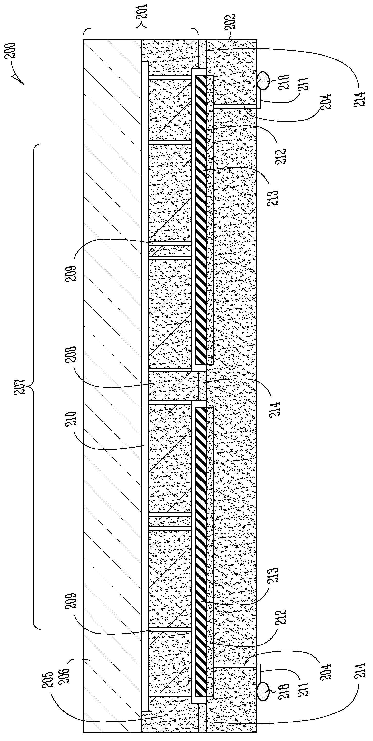
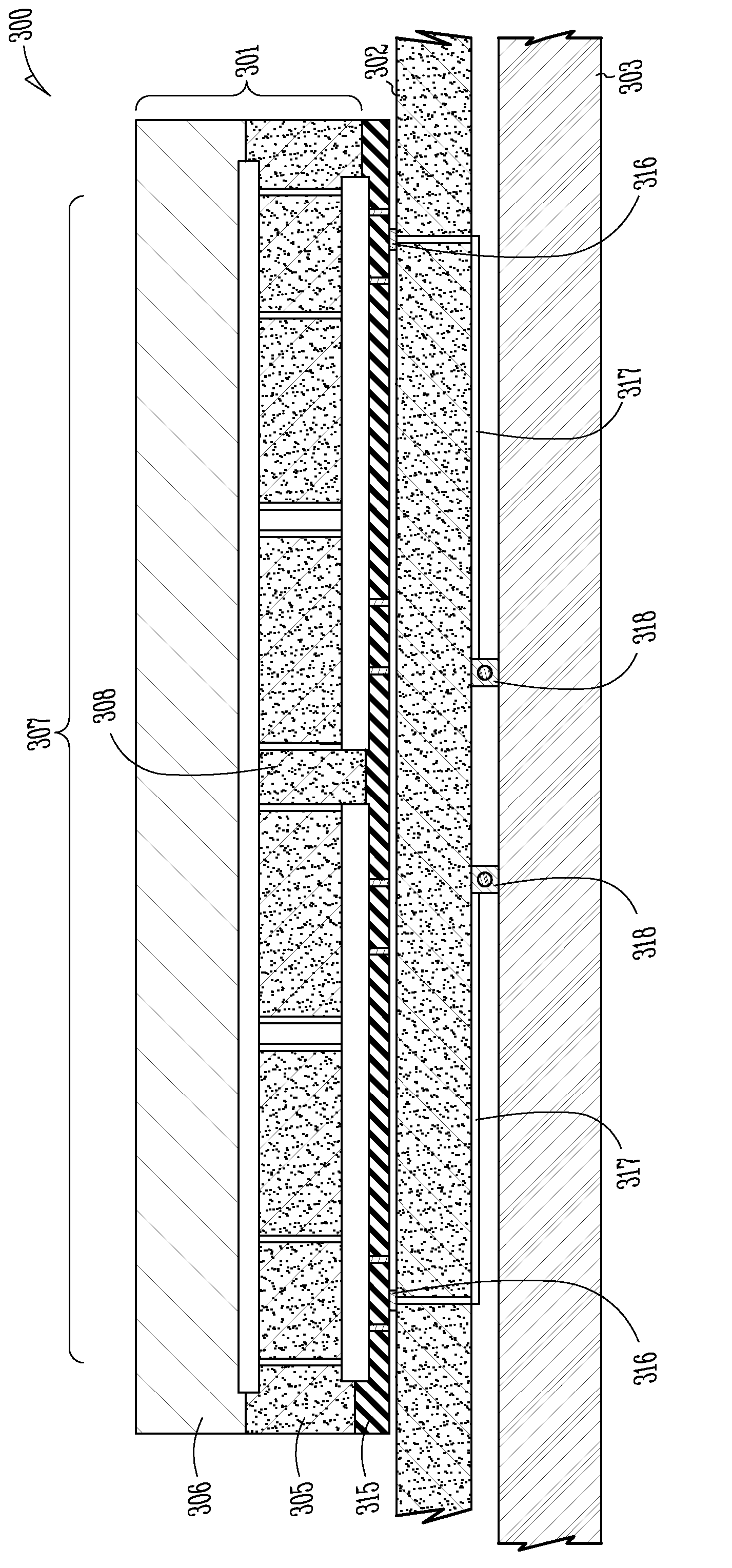
[0029] In Example 12, an apparatus can include a microelectromechanical system (MEMS) integrated circuit (IC) and a controller IC. The MEMS IC may include: a device layer having a plurality of gaps forming a plurality of movable portions and a single anchor configured to support the plurality of movable portions; and A protective layer coupled to the device layer and configured to maintain a vacuum around the plurality of movable portions and restrict out-of-plane movement of the plurality of movable portions. The controller IC has a first side coupled to the MEMS IC, and the controller IC may include a through silicon via extending through the controller IC from the first side to the the second side of the controller IC. The through-silicon vias may be configured to electrically couple contacts on the first side of the controller IC with contacts on the second side of the controller IC.
[0030] In Example 13, the MEMS IC of any one or more of Examples 1-12 optionally inclu...
PUM
 Abstract
Description
Claims
Application Information
 - R&D Engineer
- R&D Manager
- IP Professional
- Industry Leading Data Capabilities
- Powerful AI technology
- Patent DNA Extraction
Browse by: Latest US Patents, China's latest patents, Technical Efficacy Thesaurus, Application Domain, Technology Topic, Popular Technical Reports.
© 2024 PatSnap. All rights reserved.Legal|Privacy policy|Modern Slavery Act Transparency Statement|Sitemap|About US| Contact US: help@patsnap.com